TRM Name always "TE Series Name" +TRM, for example "TE0720 TRM"
...
Page properties
hidden
true
id
Comments
Important General Note:
If some section is configurable and depends on Firmware, please refer to the addition page (for example CPLD). If not available, add note, that this part is configurable
Designate all graphics and pictures with a number and a description, Use "Scroll Title" macro
Use "Scroll Title" macro for pictures and table labels. Figure number must be set manually at the moment (automatically enumeration is planned by scrollPDF)
Figure template:
Scroll Title
anchor
Figure_xanchorname
title
Figure x: Text
Scroll Ignore
Create DrawIO object here: Attention if you copy from other page, use
Scroll Only
image link to the generate DrawIO PNG file of this page. This is a workaround until scroll pdf export bug is fixed
Table template:
Layout macro can be use for landscape of large tables
Scroll Title
anchor
Table_x
title
Table x: Text
Scroll Table Layout
orientation
portrait
sortDirection
ASC
repeatTableHeaders
default
style
widths
sortByColumn
1
sortEnabled
false
cellHighlighting
true
Example
Comment
1
2
...
The anchors of the Scroll Title should be named consistant across TRMs. A incomplete list of examples is given below
<type>_<main section>_<name>
type: Figure, Table
main section:
"OV" for Overview
"SIP" for Signal Interfaces and Pins,
"OBP" for On board Peripherals,
"PWR" for Power and Power-On Sequence,
"B2B" for Board to Board Connector,
"TS" for Technical Specification
"VCP" for Variants Currently in Production
"RH" for Revision History
name: custom, some fix names, see below
Fix names:
"Figure_OV_BD" for Block Diagram
"Figure_OV_MC" for Main Components
"Table_OV_IDS" for Initial Delivery State
"Table_PWR_PC" for Power Consumption
"Figure_PWR_PD" for Power Distribution
"Figure_PWR_PS" for Power Sequence
"Figure_PWR_PM" for Power Monitoring
"Table_PWR_PR" for Power Rails
"Table_PWR_BV" for Bank Voltages
"Table_TS_AMR" for Absolute_Maximum_Ratings
"Table_TS_ROC" for Recommended_Operating_Conditions
"Figure_TS_PD" for Physical_Dimensions
"Table_VCP_SO" for TE_Shop_Overview
"Table_RH_HRH" for Hardware_Revision_History
"Table_RH_DCH" for Document_Change_History
Use Anchor in the document: add link macro and add "#<anchorname>
Refer to Anchror from external : <page url>#<pagename without space characters>-<anchorname>
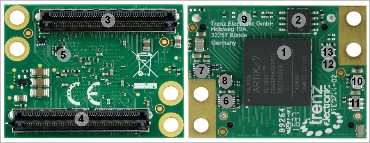
Picture of the PCB (top and bottom side) with labels of important components
Add List below
Scroll Title
anchor
Figure_OV_MC
title
Figure 2: TE0714 main components
Scroll Ignore
draw.io Diagram
border
false
viewerToolbar
true
fitWindow
false
diagramDisplayName
lbox
true
revision
2
diagramName
MC-TE0714
simpleViewer
true
width
links
auto
tbstyle
top
diagramWidth
641
Scroll Only
...
Initial Delivery State
Scroll Title
anchor
Table_InitialOV_Delivery_StateIDS
title
Table 1: Initial delivery state of programmable devices on the module.
Scroll Table Layout
orientation
portrait
sortDirection
ASC
repeatTableHeaders
default
style
widths
30%,25%,45%
sortByColumn
1
sortEnabled
false
cellHighlighting
true
Storage device name
Content
Notes
SPI Flash OTP Area
Empty, not programmed
Except serial number programmed by flash vendor
SPI Flash Quad Enable bit
Programmed
SPI Flash main array
demo design
eFUSE USER
Not programmed
eFUSE Security
Not programmed
Control Signals
Page properties
hidden
true
id
Comments
Overview of Boot Mode, Reset, Enables,
Boot process is controlled by signals on the board to board (B2B) connector.
Scroll Title
anchor
Table_BootOV_SignalsBS
title
Table 2: Boot signals.
Scroll Table Layout
orientation
portrait
sortDirection
ASC
repeatTableHeaders
default
style
widths
16%,14%,19%,51
sortByColumn
1
sortEnabled
false
cellHighlighting
true
Signal
Direction
Signal State
Description
BOOTMODE
input
high or open
Master SPI, x4 Mode
low or ground
Slave SelectMAP
PROG_B
input
pulsed low
Clear FPGA configuration (falling edge) and initiate a new configuration sequenz (next rising edge).
DONE
output
high
Completion of configuration sequence.
Note
SPI FPGA pins D02 and D03 have no pull-ups on the module, so with PUDC=High option, those pins are floating if there are no pull-ups on baseboard. As those pins have SPI RESET function when Quad mode is not enabled, it is mandatory to either add pull-ups on user baseboard or program the Quad Enable bit in Flash nonvolatile status register.
...
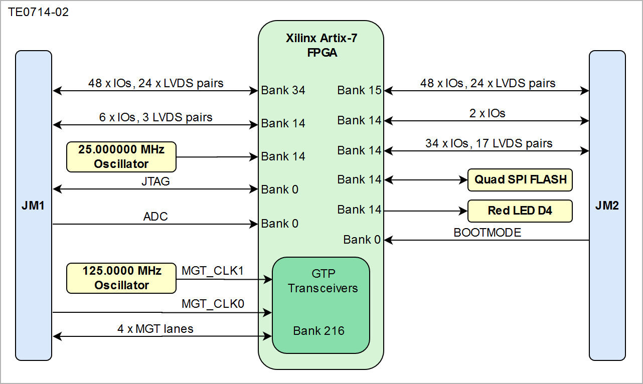
JTAG access to the Xilinx Artix-7 FPGA device is provided through connector JM1.
Scroll Title
anchor
Table_SIP_JTAG
title
Table 3: JTAG signals.
Scroll Table Layout
orientation
portrait
sortDirection
ASC
repeatTableHeaders
default
style
widths
sortByColumn
1
sortEnabled
false
cellHighlighting
true
Signal Name
B2B Pin
TCK
JM1:89
TDI
JM1:85
TDO
JM1:87
TMS
JM1:91
On-board LED
Board to Board (B2B) I/Os
FPGA bank number and number of I/O signals connected to the B2B connector:There is one LED on TE0714 module.
Scroll Title
anchor
Table_SIP_LEDsB2B
title
Table 4: LED connection.B2B I/Os
Scroll Table Layout
orientation
portrait
sortDirection
ASC
repeatTableHeaders
default
style
widths
sortByColumn
1
sortEnabled
false
cellHighlighting
true
LED
Color
FPGA
Notes
D4
Red
K18
User programmable
Clock
...
anchor
Table_Clocks
title
Table 5: Clock signals.
...
Clock
...
Default Frequency
...
IC
...
FPGA
...
Notes
...
25 MHz
...
U8
...
T14
...
125MHz
...
U2
...
B6/B5
...
Frequency depends on the module variant
style
widths
sortByColumn
1
sortEnabled
false
cellHighlighting
true
FPGA Bank
B2B Connector
I/O Signal Count
Voltage Level
Notes
14
JM1
6
VCCIO_0
14
JM2
36
VCCIO_0
NB! 17 LVDS pairs possible.
15
JM2
48
VCCIO15
Supplied by the baseboard.
34
JM1
48
VCCIO34
Supplied by the baseboard.
216
JM1
16
MGT_AVCC
MGT_AVTT
4 x GTP lanes.
Please refer to the Pin-out tables page for additional information.
On-board Peripherals
Page properties
hidden
true
id
Comments
Notes :
add subsection for every component which is important for design, for example:
Ethernet PHY
USB PHY
Programmable Clock Generator
Oscillators
eMMCs
RTC
FTDI
...
DIP-Switches
Buttons
LEDs
Quad SPI Flash
On-board SPI flash memory S25FL127S (U7) is used to store initial FPGA configuration. Besides FPGA configuration, remaining free flash memory can be used for user application storage. All four SPI data lines are connected to the FPGA allowing x1, x2 or x4 data bus widths. Maximum data rate depends on the bus width and clock frequency used.
Note
SPI Flash QE (Quad Enable) bit must be set to high or FPGA is unable to load its configuration from flash. By default this bit is set to high at the manufacturing plant.
On-board LED
There is one LED on TE0714 module.
Board to Board (B2B) I/Os
FPGA bank number and number of I/O signals connected to the B2B connector:
Scroll Title
anchor
Table_B2BOBP_LEDs
title
Table 6: B2B I/OsLED connection.
Scroll Table Layout
orientation
portrait
sortDirection
ASC
repeatTableHeaders
default
style
widths
sortByColumn
1
sortEnabled
false
cellHighlighting
true
FPGA Bank
B2B Connector
I/O Signal Count
Voltage Level
Notes
14
JM1
6
VCCIO_0
14
JM2
36
VCCIO_0
NB! 17 LVDS pairs possible.
15
JM2
48
VCCIO15
Supplied by the baseboard.
34
JM1
48
VCCIO34
Supplied by the baseboard.
216
JM1
16
MGT_AVCC
MGT_AVTT
4 x GTP lanes.
Please refer to the Pin-out tables page for additional information.
On-board Peripherals
Page properties
hidden
true
id
Comments
Notes :
add subsection for every component which is important for design, for example:
Ethernet PHY
USB PHY
Programmable Clock Generator
Oscillators
eMMCs
RTC
FTDI
...
DIP-Switches
Buttons
LEDs
Quad SPI Flash
On-board SPI flash memory S25FL127S (U7) is used to store initial FPGA configuration. Besides FPGA configuration, remaining free flash memory can be used for user application storage. All four SPI data lines are connected to the FPGA allowing x1, x2 or x4 data bus widths. Maximum data rate depends on the bus width and clock frequency used.
true
LED
Color
FPGA
Notes
D4
Red
K18
User programmable
Clock
Scroll Title
anchor
Table_OBP_Clocks
title
Clock signals.
Scroll Table Layout
orientation
portrait
sortDirection
ASC
repeatTableHeaders
default
style
widths
14%,15%,6%,9%,56%
sortByColumn
1
sortEnabled
false
cellHighlighting
true
Clock
Default Frequency
IC
FPGA
Notes
CLK25MHz
25 MHz
U8
T14
Frequency depends on the module variant. Output is compatible to 3.3V and 1.8V I/O standard of the FPGA bank.
MGT_CLK
125MHz
U2
B6/B5
Frequency depends on the module variant
Note
SPI Flash QE (Quad Enable) bit must be set to high or FPGA is unable to load its configuration from flash. By default this bit is set to high at the manufacturing plant.
Power and Power-On Sequence
...
Power Consumption
Scroll Title
anchor
Table_PowerPWR_ConsumptionPC
title
Table 7: Power Consumption
Scroll Table Layout
orientation
portrait
sortDirection
ASC
repeatTableHeaders
default
style
widths
sortByColumn
1
sortEnabled
false
cellHighlighting
true
Test Condition (25 °C ambient)
VIN Current mA
Notes
TE0714-35, TEBT0714, empty design, GT not enabled
110mA
...
Power Distribution Dependencies
Scroll Title
anchor
Figure_PWR_PD
title
Figure 3: Power Distribution
Scroll Ignore
draw.io Diagram
border
false
viewerToolbar
true
fitWindow
false
diagramDisplayName
lbox
true
revision
6
diagramName
PD-TE0714
simpleViewer
true
width
links
auto
tbstyle
top
diagramWidth
641
Scroll Only
...
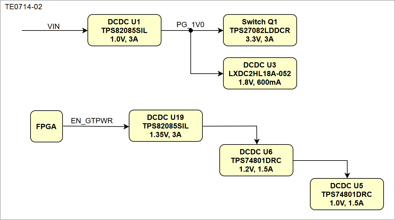
Scroll Title
anchor
Figure_PowerPWR_SequencyPS
title
Figure 4: Power-On Sequency
Scroll Ignore
draw.io Diagram
border
false
viewerToolbar
true
fitWindow
false
diagramDisplayName
lbox
true
revision
2
diagramName
TE0714-02_Power_Sequenz
simpleViewer
true
width
links
auto
tbstyle
top
diagramWidth
641
Scroll Only
Power Rails
Scroll Title
anchor
Table_PWR_Power_RailsPR
title
Table 8: Power Rails
Scroll Table Layout
orientation
portrait
sortDirection
ASC
repeatTableHeaders
default
style
widths
sortByColumn
1
sortEnabled
false
cellHighlighting
true
Voltages on B2B-
Connector
B2B JM1-Pin
B2B JM1-Pin
Direction
Note
VIN
98, 100
-
input
supply voltage
VCCIO_0
-
54
input
high range bank voltage
VCCIO_15
-
53
input
high range bank voltage
VCCIO_34
62
-
input
high range bank voltage
3.3V
84
-
output
internal 3.3V voltage level
1.8V
-
17
output
internal 1.8V voltage level
Bank Voltages
Scroll Title
anchor
Table_BankPWR_VoltagesBV
title
Table 9: Bank Voltages
Scroll Table Layout
orientation
portrait
sortDirection
ASC
repeatTableHeaders
default
style
widths
sortByColumn
1
sortEnabled
false
cellHighlighting
true
Bank
Voltage
Notes
0 Config and B14
1.8V or 3.3V
Depends on module variant
15
User
Supplied from baseboard via B2B connector, max 3.3V
34
User
Supplied from baseboard via B2B connector, max 3.3V