...
| Page properties |
|---|
|
Important General Note: |
...
| Scroll Title |
|---|
| anchor | Figure_OV_BD |
|---|
| title | TEC0850-02 block diagram |
|---|
|
| Scroll Only |
|---|
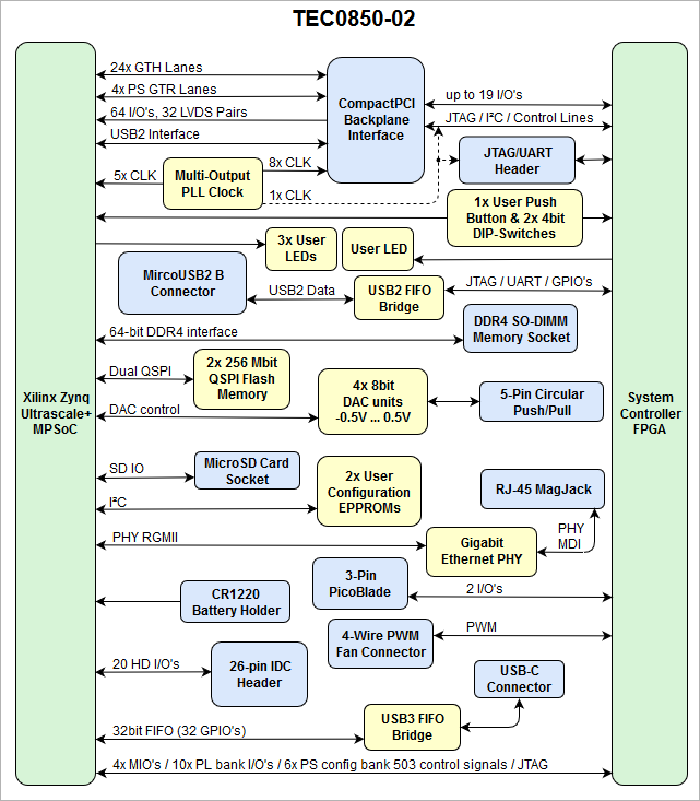 Image Added Image Added
|
| Scroll Ignore |
|---|
| draw.io Diagram |
|---|
| border | false |
|---|
| viewerToolbar | true |
|---|
| |
|---|
| fitWindow | false |
|---|
| diagramDisplayName | |
|---|
| lbox | true |
|---|
| revision | 6 |
|---|
| diagramName | TEC0850 overview |
|---|
| simpleViewer | false |
|---|
| width | |
|---|
| links | auto |
|---|
| tbstyle | hidden |
|---|
| diagramWidth | 641 |
|---|
|
| scroll-only | Image Removed |
|
Main Components
| Page properties |
|---|
|
Notes : - Picture of the PCB (top and bottom side) with labels of important components
- Add List below
|
| Scroll Title |
|---|
| anchor | Figure_OV_MC |
|---|
| title | TEC0850-02 main components |
|---|
|
| Scroll Only |
|---|
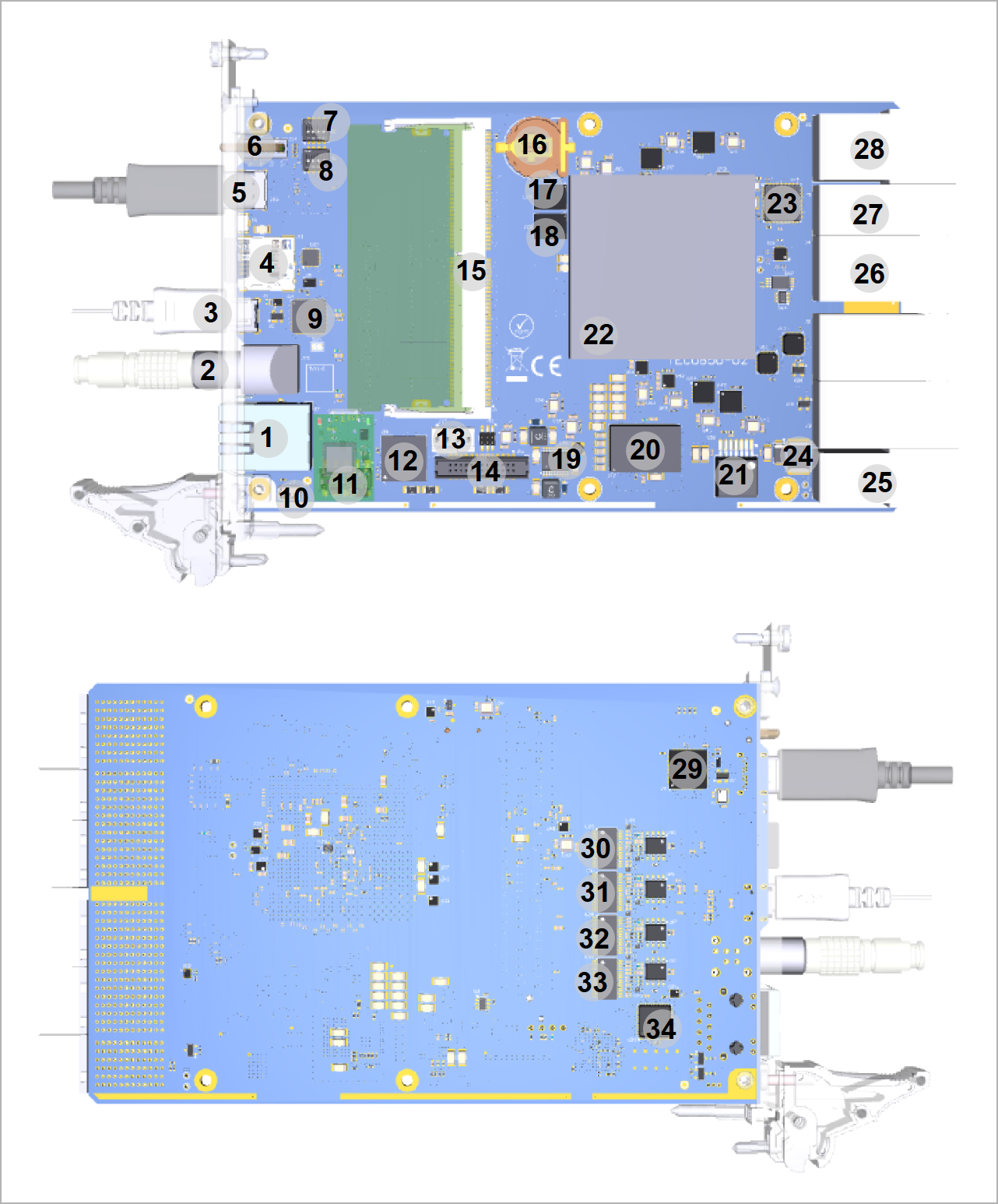 Image Added Image Added
|
| Scroll Ignore |
|---|
| draw.io Diagram |
|---|
| border | false |
|---|
| viewerToolbar | true |
|---|
| |
|---|
| fitWindow | false |
|---|
| diagramDisplayName | |
|---|
| lbox | true |
|---|
| revision | 5 |
|---|
| diagramName | TEC0850 main components |
|---|
| simpleViewer | false |
|---|
| width | |
|---|
| links | auto |
|---|
| tbstyle | hidden |
|---|
| diagramWidth | 641 |
|---|
|
| | Scroll Only |
|---|
Image Removed |
|
- GbE RJ-45 MagJack, J7
- 5-pin circular push/pull receptacle connector for DAC output, J15
- Micro USB 2.0 B receptacle connector, J9
- MicroSD Card socket, J11
- USB 3.0 Type C connector, J10
- LED light pipes J14 integrating LEDs D1 ... D4
- 4bit DIP-switch, S2
- 4bit DIP-switch, S1
- FTDI FT2232 USB 2.0 to UART/JTAG bridge, U4
- 3-pin PicoBlade header, J8
- MAX10 FPGA JTAG/UART 10-pin header, J13
- Altera MAX10 System Controller FPGA, U18
- 4-Wire PWM fan connector, J17
- 26-pin IDC header for FPGA PL I/O's, J16
- DDR4 SO-DIMM 260-pin socket, U3
- Battery Holder CR1220, B1
- 256 Mbit (32 MByte) Micron Serial NOR Flash Memory N25Q256A, U24
- 256 Mbit (32 MByte) Micron Serial NOR Flash Memory N25Q256A, U25
- DC-DC Converter LT8471IFE @+5VA/-5VA, U74
- DC-DC Converter EM2130L02QI @VCCINT_0V85, U17
- DC-DC Converter 171050601 @5V, U50
- Xilinx Zynq Ultrascale+ MPSoC, U1
- Si5345A 10-output I²C programmable PLL clock, U14
- Main power fuse @2.5A/16V, F1
- cPCI connector, J1
- cPCI connector, J4
- cPCI connector, J5
- cPCI connector, J6
- FTDI FT601Q USB 3.0 to FIFO bridge, U9
- TI THS5641 8bit DAC ,U28
- TI THS5641 8bit DAC ,U31
- TI THS5641 8bit DAC ,U29
- TI THS5641 8bit DAC ,U33
- Marvell Alaska 88E1512 GbE PHY ,U20
...
| Scroll Title |
|---|
| anchor | Figure_SIP_CompactPCI |
|---|
| title | TEC0850-02 CompactPCI I/O and high-speed interfaces |
|---|
|
| Scroll Only |
|---|
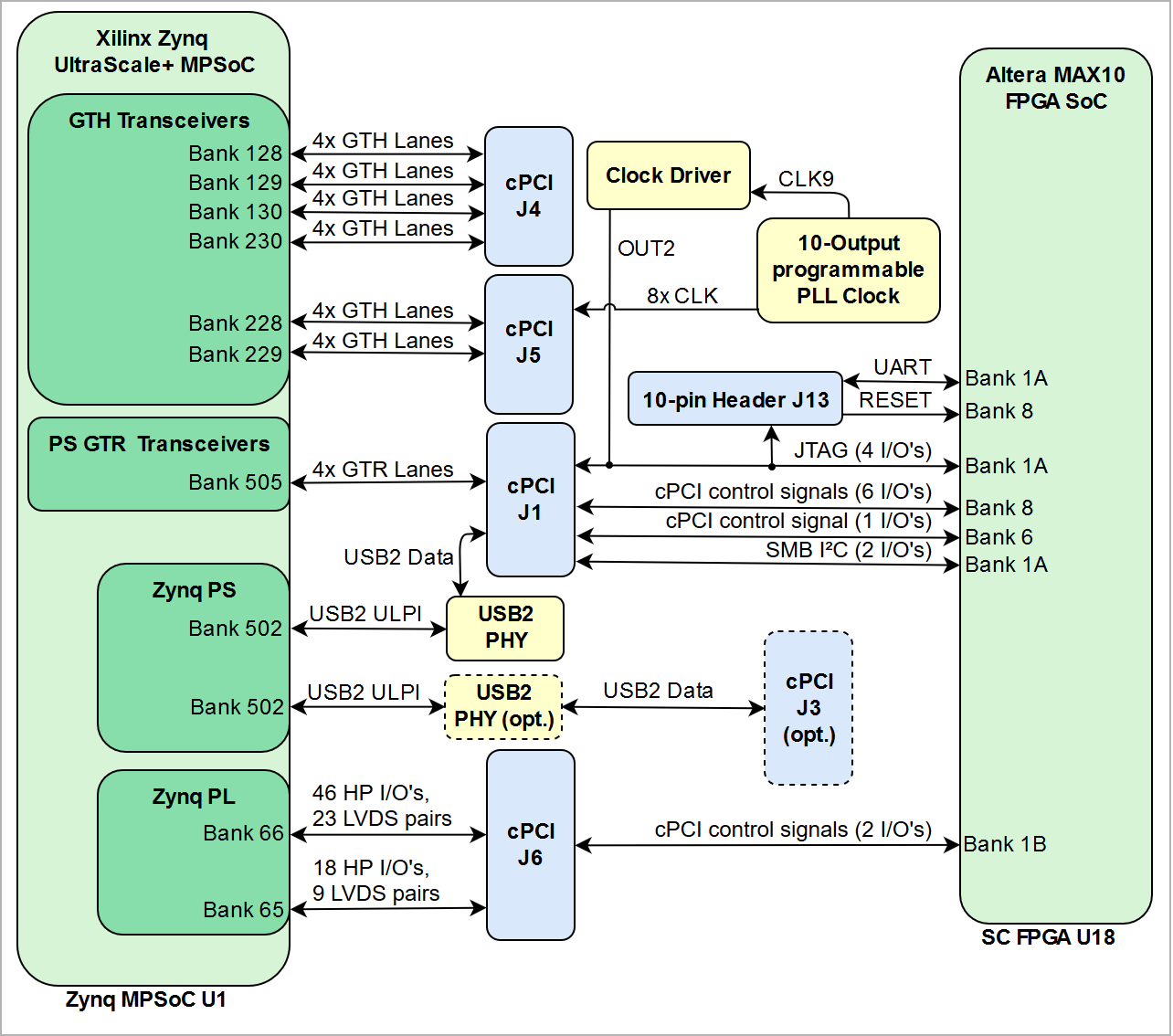 Image Added Image Added
|
| Scroll Ignore |
|---|
| draw.io Diagram |
|---|
| border | false |
|---|
| viewerToolbar | true |
|---|
| |
|---|
| fitWindow | false |
|---|
| diagramDisplayName | |
|---|
| lbox | true |
|---|
| revision | 18 |
|---|
| diagramName | IO Diagram |
|---|
| simpleViewer | false |
|---|
| width | |
|---|
| links | auto |
|---|
| tbstyle | hidden |
|---|
| diagramWidth | 642 |
|---|
|
| | Scroll Only |
|---|
Image Removed |
|
Following tables contains information about the interfaces, I/O's, clock and VCCIO sources available on the cPCI connectors:
...
| Scroll Title |
|---|
| anchor | Figure_SIP_usb3 |
|---|
| title | TEC0850-02 USB3 to FIFO bridge |
|---|
|
| Scroll Only |
|---|
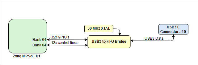 Image Added Image Added
|
| Scroll Ignore |
|---|
| draw.io Diagram |
|---|
| border | false |
|---|
| viewerToolbar | true |
|---|
| |
|---|
| fitWindow | false |
|---|
| diagramDisplayName | |
|---|
| lbox | true |
|---|
| revision | 1 |
|---|
| diagramName | TEC0850 USB2 to FIFO |
|---|
| simpleViewer | false |
|---|
| width | |
|---|
| links | auto |
|---|
| tbstyle | hidden |
|---|
| diagramWidth | 642 |
|---|
|
| | Scroll Only |
|---|
Image Removed |
|
The USB 3.0 to FIFO bridge FTDI FT601Q U9 is connected to the Zynq MPSoC's PL bank 64 and is accessible through USB-C connector J10:
...
| Scroll Title |
|---|
| anchor | Figure_SIP_jtag_uart |
|---|
| title | JTAG/UART Interface |
|---|
|
| Scroll Only |
|---|
 Image Added Image Added
|
| Scroll Ignore |
|---|
| draw.io Diagram |
|---|
| border | false |
|---|
| viewerToolbar | true |
|---|
| |
|---|
| fitWindow | false |
|---|
| diagramDisplayName | |
|---|
| lbox | true |
|---|
| revision | 8 |
|---|
| diagramName | uart_jtag |
|---|
| simpleViewer | false |
|---|
| width | |
|---|
| links | auto |
|---|
| tbstyle | hidden |
|---|
| diagramWidth | 642 |
|---|
|
| scroll-only | Image Removed |
|
The USB2 to FIFO bridge FTDI FT2232H U4 is connected to the SC FPGA U18 and is accessible through Micro-USB2 connector J9:
...
| Scroll Title |
|---|
| anchor | Figure_SIP_microsd |
|---|
| title | MicroSD Card interface |
|---|
|
| Scroll Only |
|---|
 Image Added Image Added
|
| Scroll Ignore |
|---|
| draw.io Diagram |
|---|
| border | false |
|---|
| viewerToolbar | true |
|---|
| |
|---|
| fitWindow | false |
|---|
| diagramDisplayName | |
|---|
| lbox | true |
|---|
| revision | 2 |
|---|
| diagramName | TEC0850 SD IO |
|---|
| simpleViewer | false |
|---|
| width | |
|---|
| links | auto |
|---|
| tbstyle | hidden |
|---|
| diagramWidth | 641 |
|---|
|
| | Scroll Only |
|---|
Image Removed |
|
There are some limitations to use SD card Interface in Linux.
...
| Scroll Title |
|---|
| anchor | Figure_SIP_eth |
|---|
| title | Gigabit Ethernet Interface |
|---|
|
| Scroll Only |
|---|
 Image Added Image Added
|
| Scroll Ignore |
|---|
| draw.io Diagram |
|---|
| border | false |
|---|
| viewerToolbar | true |
|---|
| |
|---|
| fitWindow | false |
|---|
| diagramDisplayName | |
|---|
| lbox | true |
|---|
| revision | 2 |
|---|
| diagramName | TEC0850 GbE |
|---|
| simpleViewer | false |
|---|
| width | |
|---|
| links | auto |
|---|
| tbstyle | hidden |
|---|
| diagramWidth | 641 |
|---|
|
| | Scroll Only |
|---|
Image Removed |
|
DDR4 SODIMM Socket
On the TEC0850 board, there is a DDR4 memory interface U3 with a 64-bit data bus width available for SO-DIMM modules connected to the Zynq UltraScale+ DDRC hard memory controller.
| Scroll Title |
|---|
| anchor | Figure_SIP_ddr4 |
|---|
| title | DDR4 SDRAM SODIMM socket |
|---|
|
| Scroll Only |
|---|
 Image Added Image Added
|
| Scroll Ignore |
|---|
| draw.io Diagram |
|---|
| border | false |
|---|
| viewerToolbar | true |
|---|
| |
|---|
| fitWindow | false |
|---|
| diagramDisplayName | |
|---|
| lbox | true |
|---|
| revision | 1 |
|---|
| diagramName | TEC0850 DDR4 interface |
|---|
| simpleViewer | false |
|---|
| width | |
|---|
| links | auto |
|---|
| tbstyle | hidden |
|---|
| diagramWidth | 641 |
|---|
|
| | Scroll Only |
|---|
Image Removed |
|
Following table gives an overview of the memory interface I/O signals of the DDR4 SDRAM SO-DIMM Socket U3:
...
| Scroll Title |
|---|
| anchor | Figure_SIP_dac |
|---|
| title | 4x 8bit DAC units |
|---|
|
| Scroll Only |
|---|
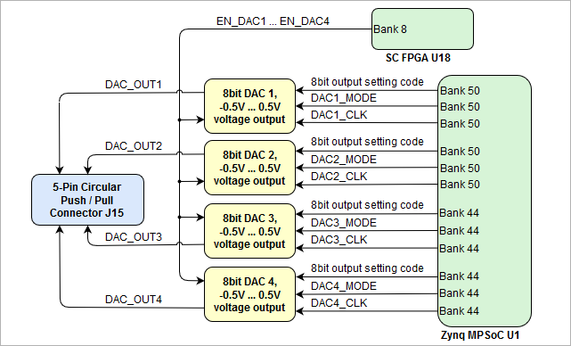 Image Added Image Added
|
| Scroll Ignore |
|---|
| draw.io Diagram |
|---|
| border | false |
|---|
| viewerToolbar | true |
|---|
| |
|---|
| fitWindow | false |
|---|
| diagramDisplayName | |
|---|
| lbox | true |
|---|
| revision | 3 |
|---|
| diagramName | TEC0850 DACs |
|---|
| simpleViewer | false |
|---|
| width | |
|---|
| links | auto |
|---|
| tbstyle | hidden |
|---|
| diagramWidth | 641 |
|---|
|
| | Scroll Only |
|---|
Image Removed |
|
There is a 26-pin IDC header (2x13, 1.27mm grid size) J16 available on the TEC0850 board which exposes the 20 FPGA HD I/O's of PL bank 47 to the user. The PL bank 47 has 3.3V VCCO bank voltage, on the header J16 there also the voltage levels 3.3V and 5V available. The I/O's can be accessed with a corresponding IDC connector.
| Scroll Title |
|---|
| anchor | Figure_SIP_idc_mpsoc_pl |
|---|
| title | Zynq MPSoC PL I/O's IDC pin-header |
|---|
|
| Scroll Only |
|---|
 Image Added Image Added
|
| Scroll Ignore |
|---|
| draw.io Diagram |
|---|
| border | false |
|---|
| viewerToolbar | true |
|---|
| |
|---|
| fitWindow | false |
|---|
| diagramDisplayName | |
|---|
| lbox | true |
|---|
| revision | 3 |
|---|
| diagramName | TEC0850 header J16 |
|---|
| simpleViewer | false |
|---|
| width | |
|---|
| links | auto |
|---|
| tbstyle | hidden |
|---|
| diagramWidth | 641 |
|---|
|
| | Scroll Only |
|---|
Image Removed |
|
On the TEC0850 there is a 10-pin SMT header (2x5, 2.54mm grid size) J13 present which provides access to the JTAG and UART interface of Altera MAX10 System Controller FPGA. The header J13 has a compatible pin assignment to the TEI0004 JTAG programmer for Altera FPGAs, the voltage levels 3.3V is on the header available as a reference I/O-voltage for JTAG and UART.
...
| Scroll Title |
|---|
| anchor | Figure_SIP_10pin_jtag_uart |
|---|
| title | 10-pin JTAG/UART header |
|---|
|
| Scroll Only |
|---|
 Image Added Image Added
|
| Scroll Ignore |
|---|
| draw.io Diagram |
|---|
| border | false |
|---|
| viewerToolbar | true |
|---|
| |
|---|
| fitWindow | false |
|---|
| diagramDisplayName | |
|---|
| lbox | true |
|---|
| revision | 3 |
|---|
| diagramName | TEC0850 header 13 |
|---|
| simpleViewer | false |
|---|
| width | |
|---|
| links | auto |
|---|
| tbstyle | hidden |
|---|
| diagramWidth | 641 |
|---|
|
| | Scroll Only |
|---|
Image Removed |
|
2 I/O's of the SC FPGA U18 are exposed to the on-board 3-Pin PicoBlade header J8 available to the user or for future use of upcoming versions of SC FPGA firmware.
| Scroll Title |
|---|
| anchor | Figure_SIP_3pin_picoblade |
|---|
| title | 3-pin PicoBlade header |
|---|
|
| Scroll Only |
|---|
 Image Added Image Added
|
| Scroll Ignore |
|---|
| draw.io Diagram |
|---|
| border | false |
|---|
| viewerToolbar | true |
|---|
| |
|---|
| fitWindow | false |
|---|
| diagramDisplayName | |
|---|
| lbox | true |
|---|
| revision | 1 |
|---|
| diagramName | TEC0850 3-pin header J8 |
|---|
| simpleViewer | false |
|---|
| width | |
|---|
| links | auto |
|---|
| tbstyle | hidden |
|---|
| diagramWidth | 641 |
|---|
|
| | Scroll Only |
|---|
Image Removed |
|
Battery Holder
There is a CR1220 battery holder available to the supply the voltage for the Zynq MPSoC's Battery Power Domain (BBRAM and RTC). The battery voltage VBATT should be in the range of 2.2V to 5.5V, use the 3.0V CR1220 battery.
| Scroll Title |
|---|
| anchor | Figure_SIP_Battery_Holder |
|---|
| title | Backup-Battery Holder |
|---|
|
| Scroll Only |
|---|
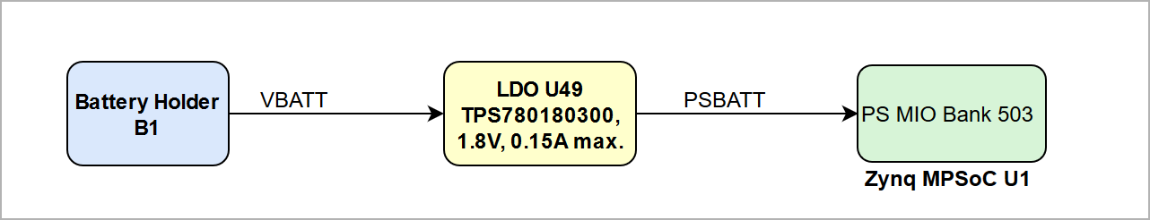 Image Added Image Added
|
| Scroll Ignore |
|---|
| draw.io Diagram |
|---|
| border | false |
|---|
| viewerToolbar | true |
|---|
| |
|---|
| fitWindow | false |
|---|
| diagramDisplayName | |
|---|
| lbox | true |
|---|
| revision | 4 |
|---|
| diagramName | TEC0850 battery holder |
|---|
| simpleViewer | false |
|---|
| width | |
|---|
| links | auto |
|---|
| tbstyle | hidden |
|---|
| diagramWidth | 641 |
|---|
|
| | Scroll Only |
|---|
Image Removed |
|
4-Wire PWM FAN Connectors
...
| Scroll Title |
|---|
| anchor | Figure_SIP_fan |
|---|
| title | 4-wire PWM FAN connector |
|---|
|
| scroll-only |
|---|
 Image Added Image Added
|
| scroll-ignore |
|---|
| draw.io Diagram |
|---|
| border | false |
|---|
| viewerToolbar | true |
|---|
| |
|---|
| fitWindow | false |
|---|
| diagramDisplayName | |
|---|
| lbox | true |
|---|
| revision | 2 |
|---|
| diagramName | TEC0850 4-Wire PWM Connector |
|---|
| simpleViewer | false |
|---|
| width | |
|---|
| links | auto |
|---|
| tbstyle | hidden |
|---|
| diagramWidth | 641 |
|---|
|
|
| Scroll Only |
|---|
Image Removed |
|
Onboard Peripherals
| Page properties |
|---|
|
Notes : - add a subsection for every component which is important for design, for example:
- Ethernet PHY
- USB PHY
- Programmable Clock Generator
- Oscillators
- eMMCs
- RTC
- FTDI
- ...
- DIP-Switches
- Buttons
- LEDs
|
...
| Scroll Title |
|---|
| anchor | Figure_OBP_max10_sc |
|---|
| title | TEC0850 MAX10 System Controller FPGA |
|---|
|
| Scroll Only |
|---|
 Image Added Image Added
|
| Scroll Ignore |
|---|
| draw.io Diagram |
|---|
| border | false |
|---|
| viewerToolbar | true |
|---|
| |
|---|
| fitWindow | false |
|---|
| diagramDisplayName | |
|---|
| lbox | true |
|---|
| revision | 2 |
|---|
| diagramName | TEC0850 SC TO Zynq connections |
|---|
| simpleViewer | false |
|---|
| width | |
|---|
| links | auto |
|---|
| tbstyle | hidden |
|---|
| diagramWidth | 641 |
|---|
|
|
| Scroll Only |
|---|
Image Removed |
|
Programmable Clock Generator
...
| Scroll Title |
|---|
| anchor | Figure_OBP_si5345 |
|---|
| title | 10-output I²C programmable clock generator |
|---|
|
| scroll-only |
|---|
 Image Added Image Added
|
| scroll-ignore |
|---|
| draw.io Diagram |
|---|
| border | false |
|---|
| viewerToolbar | true |
|---|
| |
|---|
| fitWindow | false |
|---|
| diagramDisplayName | |
|---|
| lbox | true |
|---|
| revision | 5 |
|---|
| diagramName | TEC0850 clock sourdes |
|---|
| simpleViewer | false |
|---|
| width | |
|---|
| links | auto |
|---|
| tbstyle | hidden |
|---|
| diagramWidth | 641 |
|---|
|
| scroll-only | Image Removed |
|
Following table shows onboard Silicon Labs I2C programmable Si5345A U17 10-output programmable PLL reference clock generator inputs and outputs:
...
| Scroll Title |
|---|
| anchor | Figure_OBP_ft2232 |
|---|
| title | TEC0850 on-board FTDI chips |
|---|
|
| scroll-only |
|---|
 Image Added Image Added
|
| scroll-ignore |
|---|
| draw.io Diagram |
|---|
| border | false |
|---|
| viewerToolbar | true |
|---|
| |
|---|
| fitWindow | false |
|---|
| diagramDisplayName | |
|---|
| lbox | true |
|---|
| revision | 4 |
|---|
| diagramName | TEC0850 FT2232H |
|---|
| simpleViewer | false |
|---|
| width | |
|---|
| links | auto |
|---|
| tbstyle | hidden |
|---|
| diagramWidth | 641 |
|---|
|
|
| Scroll Only |
|---|
Image Removed |
|
FT2232H
The TEC0850 board is equipped with the FTDI FT2232H USB2 to JTAG/UART adapter controller connected to micro-USB2 connector J9 to provide JTAG and UART access to the Xilinx UltraScale+ Zynq SoC or Intel MAX10 (switchable over DIP) . There is also a 256-byte configuration EEPROM U6 wired to the FT2232H chip via Microwire bus which holds pre-programmed license code to support Xilinx programming tools. Refer to the FTDI datasheet to get information about the capacity of the FT2232H chip.
...
| Scroll Title |
|---|
| anchor | Figure_OBP_qspi |
|---|
| title | Quad-SPI Flash Memory |
|---|
|
| Scroll Only |
|---|
 Image Added Image Added
|
| Scroll Ignore |
|---|
| draw.io Diagram |
|---|
| border | false |
|---|
| viewerToolbar | true |
|---|
| |
|---|
| fitWindow | false |
|---|
| diagramDisplayName | |
|---|
| lbox | true |
|---|
| revision | 1 |
|---|
| diagramName | TEC0850 QSPI Flash |
|---|
| simpleViewer | false |
|---|
| width | |
|---|
| links | auto |
|---|
| tbstyle | hidden |
|---|
| diagramWidth | 641 |
|---|
|
|
|
| scroll- |
|---|
onlyImage Removed |
| scroll-title |
|---|
| anchor | Table_OBP_QSPI_FLASH |
|---|
| title | Quad-SPI Flash memory interface connections |
|---|
|
| Scroll Table Layout |
|---|
| orientation | portrait |
|---|
| sortDirection | ASC |
|---|
| repeatTableHeaders | default |
|---|
| style | |
|---|
| widths | |
|---|
| sortByColumn | 1 |
|---|
| sortEnabled | false |
|---|
| cellHighlighting | true |
|---|
|
| IC | Memory Density | MIO | Signal Schematic Name | Flash Memory Pin |
|---|
QSPI Flash U24, N25Q256A11E1240E | 256 Mbit (32 MByte) | 0 | MIO0 | B2 | | 1 | MIO1 | D2 | | 2 | MIO2 | C4 | | 3 | MIO3 | D4 | | 4 | MIO4 | D3 | | 5 | MIO5 | C2 | QSPI Flash U25, N25Q256A11E1240 | 256 Mbit (32 MByte) | 7 | MIO7 | C2 | | 8 | MIO8 | D3 | | 9 | MIO9 | D2 | | 10 | MIO10 | C4 | | 11 | MIO11 | D4 | | 12 | MIO12 | B2 |
|
...
| Scroll Title |
|---|
| anchor | Figure_OBP_eeprom |
|---|
| title | On-board configuration EEPROMs |
|---|
|
| Scroll Only |
|---|
 Image Added Image Added
|
| Scroll Ignore |
|---|
| draw.io Diagram |
|---|
| border | false |
|---|
| viewerToolbar | true |
|---|
| |
|---|
| fitWindow | false |
|---|
| diagramDisplayName | |
|---|
| lbox | true |
|---|
| revision | 2 |
|---|
| diagramName | TEC0850 USB3 to FIFO |
|---|
| simpleViewer | false |
|---|
| width | |
|---|
| links | auto |
|---|
| tbstyle | hidden |
|---|
| diagramWidth | 641 |
|---|
|
| scroll-only | Image Removed |
|
The EEPROMs U63 and U64 are programmable via the onboard I²C bus connected to MIO 20...21 pins. The I²C address is shown in the table below.
...
| Scroll Title |
|---|
| anchor | Figure_OBP_usb2_phy |
|---|
| title | TEC0850 cPCI USB2 interface |
|---|
|
| scroll-only |
|---|
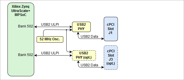 Image Added Image Added
|
| scroll-ignore |
|---|
| draw.io Diagram |
|---|
| border | false |
|---|
| viewerToolbar | true |
|---|
| |
|---|
| fitWindow | false |
|---|
| diagramDisplayName | |
|---|
| lbox | true |
|---|
| revision | 2 |
|---|
| diagramName | TEC0850 USB2 PHY |
|---|
| simpleViewer | false |
|---|
| width | |
|---|
| links | auto |
|---|
| tbstyle | hidden |
|---|
| diagramWidth | 641 |
|---|
|
| | Scroll Only |
|---|
Image Removed |
|
| Scroll Title |
|---|
| anchor | Table_OBP_usb2_phy_io |
|---|
| title | USB2 ULPI interface description |
|---|
|
| Scroll Table Layout |
|---|
| orientation | portrait |
|---|
| sortDirection | ASC |
|---|
| repeatTableHeaders | default |
|---|
| style | |
|---|
| widths | |
|---|
| sortByColumn | 1 |
|---|
| sortEnabled | false |
|---|
| cellHighlighting | true |
|---|
|
| USB2 PHY U11 Pin | Connected to | Notes |
|---|
| ULPI | PS bank MIO52 ... MIO63 | Zynq Ultrascale+ USB0 MIO pins are connected to the PHY | | REFCLK | - | 52MHz from onboard oscillator U12 | | REFSEL[0..2] | - | All pins set to GND selects the external reference clock frequency (52.000000 MHz) | | RESETB | Zynq MPSoC MIO16, pin AM16 | Low active USB2 PHY Reset
| | DP, DM | cPCI connector J1 | USB2 data lane | | CPEN | - | External USB power switch active-high enable signal | | VBUS | 5V | Connected to onboard 5V voltage level via a series of resistors, see schematic | | ID | 3.3V | USB2 OTG A-Device (host) | | optional USB2 PHY U13 Pin | Connected to | Notes |
|---|
| ULPI | PS bank MIO64 ... MIO75 | Zynq Ultrascale+ USB1 MIO pins are connected to the PHY | | REFCLK | - | 52MHz from onboard oscillator U12 | | REFSEL[0..2] | - | All pins set to GND selects the external reference clock frequency (52.000000 MHz) | | RESETB | Zynq MPSoC MIO17, pin AP16 | Low active USB2 PHY Reset | | DP, DM | optional cPCI connector J3 | USB2 data lane | | CPEN | - | External USB power switch active-high enable signal | | VBUS | 5V | Connected to onboard 5V voltage level via a series of resistors, see schematic | | ID | 3.3V | USB2 OTG A-Device (host) |
|
...
| Scroll Title |
|---|
| anchor | Figure_OBP_eth_phy |
|---|
| title | TEC0850 GbE interface with RJ-45 MegJack |
|---|
|
| scroll-only |
|---|
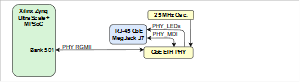 Image Added Image Added
|
| scroll-ignore |
|---|
| draw.io Diagram |
|---|
| border | false |
|---|
| viewerToolbar | true |
|---|
| |
|---|
| fitWindow | false |
|---|
| diagramDisplayName | |
|---|
| lbox | true |
|---|
| revision | 1 |
|---|
| diagramName | TEC0850 GbE PHY |
|---|
| simpleViewer | false |
|---|
| width | |
|---|
| links | auto |
|---|
| tbstyle | hidden |
|---|
| diagramWidth | 641 |
|---|
|
|
| Scroll Only |
|---|
Image Removed |
|
8bit DACs
The TEC0850 Board has 4 8-bit parallel Texas Instruments THS5641AIPW digital to analog converter (DAC) with up to 100 MSPS update rate connected to TI THS4631D operational amplifiers. See Schematic circuitry and TI THS5641 data sheet for proper operation of the on-board DAC units.
...
| Scroll Title |
|---|
| anchor | Figure_PWR_PD |
|---|
| title | Power Distribution |
|---|
|
| Scroll Only |
|---|
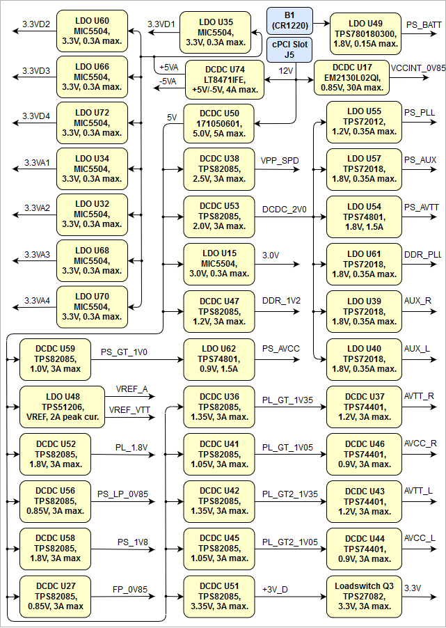 Image Added Image Added
|
| Scroll Ignore |
|---|
| draw.io Diagram |
|---|
| border | false |
|---|
| viewerToolbar | true |
|---|
| |
|---|
| fitWindow | false |
|---|
| diagramDisplayName | |
|---|
| lbox | true |
|---|
| revision | 16 |
|---|
| diagramName | Power supply |
|---|
| simpleViewer | false |
|---|
| width | |
|---|
| links | auto |
|---|
| tbstyle | hidden |
|---|
| diagramWidth | 641 |
|---|
|
|
| Scroll Only |
|---|
Image Removed |
|
Power-On Sequence
The TEC0850 board meets the recommended criteria to power up the Xilinx Zynq UltraScale+ MPSoC properly by keeping a specific sequence of enabling the onboard DC-DC converters dedicated to the particular Power Domains and powering up the onboard voltages.
...
| Scroll Title |
|---|
| anchor | Figure_PWR_PS |
|---|
| title | Power-On Sequence Diagram |
|---|
|
| scroll-only |
|---|
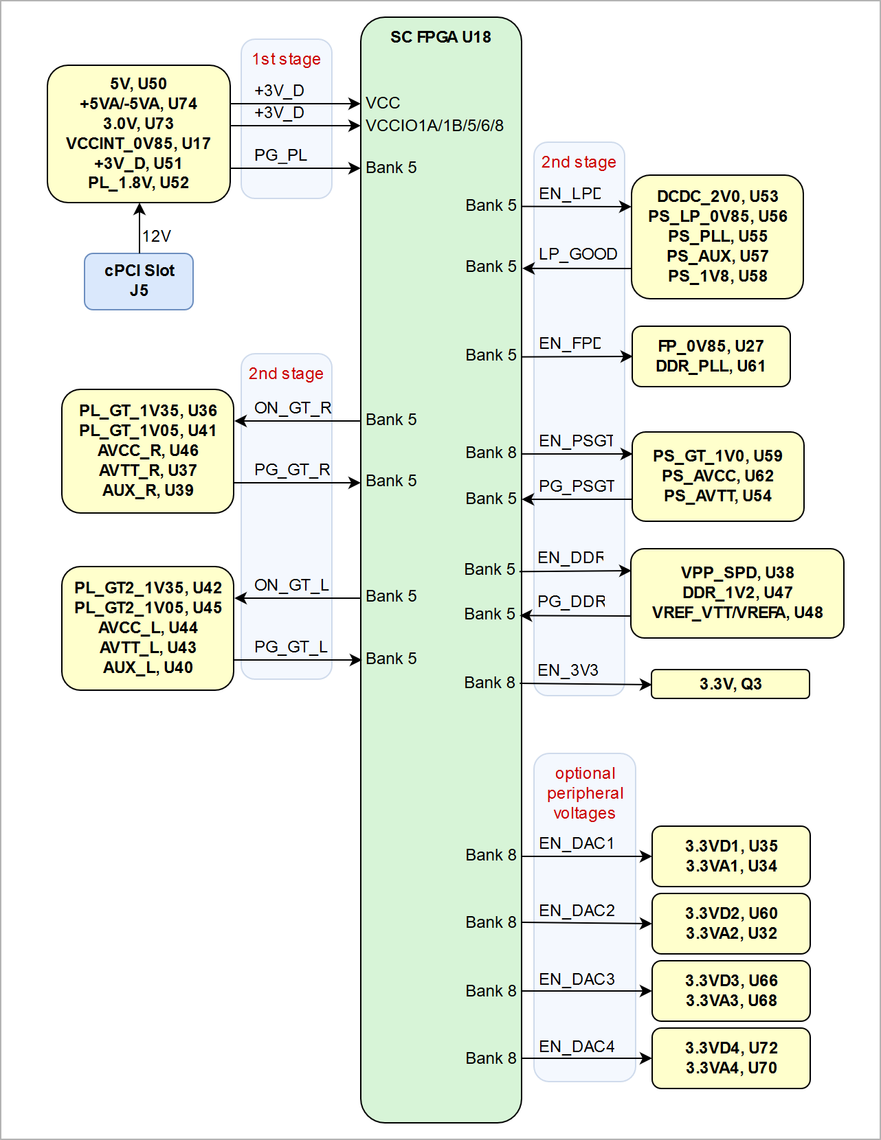 Image Added Image Added
|
| scroll-ignore |
|---|
| draw.io Diagram |
|---|
| border | false |
|---|
| viewerToolbar | true |
|---|
| |
|---|
| fitWindow | false |
|---|
| diagramDisplayName | |
|---|
| lbox | true |
|---|
| revision | 2 |
|---|
| diagramName | TEC0850 Power-On Sequence Diagram |
|---|
| simpleViewer | false |
|---|
| width | |
|---|
| links | auto |
|---|
| tbstyle | hidden |
|---|
| diagramWidth | 641 |
|---|
|
| | Scroll Only |
|---|
Image Removed |
|
| Warning |
|---|
| To avoid any damage to the MPSoC module, check for stabilized onboard voltages in a steady state before powering up the MPSoC's I/O bank voltages VCCOx. All I/Os should be tri-stated during the power-on sequence. |
...
| Scroll Title |
|---|
| anchor | Figure_PWR_PM |
|---|
| title | TEC0850 voltage Voltage monitor circuit |
|---|
|
| scroll-only |
|---|
 Image Added Image Added
|
| scroll-ignore |
|---|
| draw.io Diagram |
|---|
| border | false |
|---|
| viewerToolbar | true |
|---|
| |
|---|
| fitWindow | false |
|---|
| diagramDisplayName | |
|---|
| lbox | true |
|---|
| revision | 1 |
|---|
| diagramName | TEC0850 Voltage Monitor Circuit |
|---|
| simpleViewer | false |
|---|
| width | |
|---|
| links | auto |
|---|
| tbstyle | hidden |
|---|
| diagramWidth | 642 |
|---|
|
| | Scroll Only |
|---|
Image Removed |
|
Power Rails
| Scroll Title |
|---|
| anchor | Table_PWR_PR |
|---|
| title | TEC0850 power rails description |
|---|
|
| Scroll Table Layout |
|---|
| orientation | portrait |
|---|
| sortDirection | ASC |
|---|
| repeatTableHeaders | default |
|---|
| style | |
|---|
| widths | |
|---|
| sortByColumn | 1 |
|---|
| sortEnabled | false |
|---|
| cellHighlighting | true |
|---|
|
| Connector / Pin | Voltage | Direction | Notes |
|---|
| J1, pin A1, D1, E1, G1, H1, J1, K1 | VIN_12V | Input | Main power supply pins | | J17, pin 2 | 12V | Output | 4-wire PWM fan connector supply voltage | | J13, pin 4 | +3V_D | Output | JTAG/UART reference VCCIO voltage | | B1, pin + | VBATT | Input | 3.0V CR1220 battery | | J16, pin 2 | 5V | Output | I/O header VCCIO | | J16, pin 1 | 3.3V | Output | I/O header VCCIO | | J9, pin 4 | VBUS | Input | USB2 VBUS (5.0V nominal) | | J10, pin A4, B9 | VBUS30 | Input | USB3 VBUS (5.0V nominal) | | J11, pin 4 | 3.3V | Output | MicroSD Card VDD | | J15, pin 2 | DAC1_OUT | Output | DAC output | | J15, pin 3 | DAC2_OUT | Output | DAC output | | J15, pin 4 | DAC3_OUT | Output | DAC output | | J15, pin 5 | DAC4_OUT | Output | DAC output |
|
...