...
Carrier for 4x5 modules
LPC FMC
- SFP+ Connectorconnector
- PCIe x1
- SATA connector
- RJ45 Gigabit Ethernet connector
- micro-usb to JTAG/UART bridge
- 2x Firefly connectors
- micro usb connector
- micro SD card connector
- 4 LEDS, 4x LED (2User, Power and Status LED)
- Module reset button
- 10x user dip, 9 xfor configuration, one user
MAX10 CPLD
Block Diagram
| Scroll Title |
|---|
| anchor | Figure_OV_BD |
|---|
| title | TE... block diagram |
|---|
|
| Scroll Ignore |
|---|
| draw.io Diagram |
|---|
| border | false |
|---|
| viewerToolbar | true |
|---|
| |
|---|
| fitWindow | false |
|---|
| diagramDisplayName | |
|---|
| lbox | true |
|---|
| revision | 34 |
|---|
| diagramName | BD_TEF1002-01 |
|---|
| simpleViewer | false |
|---|
| width | |
|---|
| links | auto |
|---|
| tbstyle | top |
|---|
| diagramWidth | 633 |
|---|
|
|
| Scroll Only |
|---|
|
|
...
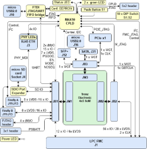
- ANSI/VITA 57.1 compliant FMC LPC connector, J1
- Cooling fan 5VDC M1 (45X5MM, 0.7W, 1.06CFM), M1
- SFP+ connector, J12
- PCIe x1 connector, J3
- SATA connector, J31
- Trenz Electronic 4 x 5 modules B2B connectors, JB1 ... JB3
- RJ45 Gigabit Ethernet connector, J9
- 2x Firefly arrangement of connectors, J11, J13, J14, J18
- Micro-USB2 connector, J10
- FTDI FT2232H USB2 to JTAG,UART/FIFO Bridge, U4
- Micro-USB2 connector, J16
- MAX10 10M08SAU169C8G CPLD, U11
- 6-pin 12V power connector, J15
- 6x1 JTAG pin header (not fitted)
- 3x1 jumper pin header (select VCCIOA), J4
- 3x1 jumper pin header (select VCCA_SD), J7
- 2x1 pin header (VBAT), J6
- 2x5 1,27mm pitch pin header (PJTAG), J19
- Push button, S1
- 10x dip switch, S2, S3
- DCDC LMZ23605TZ @5.0V (5V0PER), U15
- DCDC LMZ23605TZ @5.0V (5V0), U9
- DCDC LMZ23605TZ @3.3V(3V3IN), U10
- 2x green LED (user), D1, D2
- green LED (Power), D3
- green LED (Status), D4
- SD-Card connector (top loader),
- DCDC EN5335QI (FMC_VADJ), U1
- DCDC EN6338QI @3.3V (3V3FMC), U14
- SDIO Level shifter TXS02612, U3
...
| Scroll Title |
|---|
| anchor | Table_OV_CS |
|---|
| title | TEF1002 Control Signals |
|---|
|
| Scroll Table Layout |
|---|
| orientation | portrait |
|---|
| sortDirection | ASC |
|---|
| repeatTableHeaders | default |
|---|
| style | |
|---|
| widths | |
|---|
| sortByColumn | 1 |
|---|
| sortEnabled | false |
|---|
| cellHighlighting | true |
|---|
|
Control signal | Switch / Button / LED / Pin | Signal Schematic Names | Connected to | Functionality | Notes |
|---|
JTAG Enable | DIP switch S2-4 | | FMC_VADJ voltage selection | DIP switches S2-1, S2-2, S2-3 | VID0 ... VID2 |
JTAGEN, pin E5OFF: SC CPLD JTAG enabled,
ON: Module/FMC JTAG enabled | - | TODO!!!!!| , pins K6, J5, K5 | sets adjustable voltage for FMC connector | dependens on SC CPLD configuration | | JTAG enable | DIP switch S2-4 |
BOOT MODE U14 27MODE | B2B JB1, pin 31 | | E5 | OFF: TEF1002 SC CPLD JTAG enabled,
ON: Module/FMC JTAG enabled |
Boot Mode for attached module (Flash or SD) ResetSC CPLD U14, pin 13 | RESIN | B2B JB2, pin 17 | Module Reset | - | | Global Reset input | Push Button S2 | S2 | SC CPLD U14, pin 2 | Manual reset from user | - | | SD Card detection | SD Slot J8, pin 10 | SD_DETECT | SC CPLD U14, pin 40 | Detection Signal for inserted SD Card | Boot mode is set to SD Boot,
when SD Card is detected. | | Board status indicators | Red LEDs D1 ... D8 | ULED1 ... ULED8 | SC CPLD U14, pins
78, 77, 76, 16, 69, 68, 65, 64 | indicating various board and
module status / configuration | Refer to the firmware documentation of the SC CPLD
U14 and to the subsection 'LEDs' in section 'On-board Peripherals'
for more details and current functionality. | | Board 3.3V power indicator | Green LED D22 | 3V3IN | B2B JB1, pin 14, 16 | ON: 3.3V on-board voltage available | - | | FMC_VADJ voltage selection | DIP switches S4-1, S4-2, S4-3 | VID0 ... VID2 | SC CPLD U14, pins 34, 35, 38 | sets adjustable voltage for FMC connector | - | | I²C control / FMC_VADJ voltage selection | DIP switches S3-2, S3-1 | CM0, CM1 | SC CPLD U14, pins 99, 1 | enabling / disabling I²C control of board functionalities,
sets FMC_VADJ voltage (only 3 steps),
available to user if FMC_VADJ set by DIP-switch S4 | Refer to the firmware documentation of the SC CPLD
U14 and and to the subsection 'DIP switches' in section 'On-board
Peripherals' for current functionality and more details. | |
Signals, Interfaces and Pins
| Page properties |
|---|
|
Notes : - For carrier or stand-alone boards use subsection for every connector typ (add designator on description, not on the subsection title), for example:
- For modules which needs carrier us only classes and refer to B2B connector if more than one is used, for example
|
...
| JTAG select | DIP switch S2-5 | M_JTAGEN | B2B JB1, pin 90 | When S2-4 ON and S2-6 OFF: OFF: Module SC CPLD JTAG enabled, ON: Module SOC JTAG enabled | - | | FMC JTAG select | DIP switch S2-6 | FMC_JTAG | SC CPLD U11,L3 | When S2-4 ON: OFF: TEF1002 SC CPLD JTAG enabled, ON: FMC JTAG enabled | dependens on SC CPLD configuration, only avialiable when 4x5 module installed | | Enable module power | DIP switch S2-7 | CM0 | SC CPLD U11, M3 | Module power. Set ON to enable module power. (Power management depends on module. ) | dependens on SC CPLD configuration, only avialiable when 4x5 module installed | | No sequenzing | DIP switch S2-8 | CM1 | SC CPLD U11, L2 | Module Power management. Set ON to disable module CPLD power management. Power management depends on module and not all modules support extended power management with CPLD. | dependens on SC CPLD configuration, only avialiable when 4x5 module installed | | Boot Mode | DIP switch S3-1 | CM2 | SC CPLD U11, K2 | Boot Mode for attached module (Default: OFF for primary SD boot and ON for primary QSPI boot. Depends also on module CPLD firmware). | dependens on SC CPLD configuration, only avialiable when 4x5 module installed | | FMC VADJ enable | DIP switch S3-2 | USR0 | SC CPLD U11, K1 | ON: FMC VADJ enable also without installed FMC Card OFF: FMC_FADJ only enabled when FMC installed. | dependens on SC CPLD configuration, only avialiable when 4x5 module installed | | Reset | Push button S1 | BUTTON | SC CPLD U11, N6 | Module Reset, Low active module reset. Pin force Power one reset on FPGA/SoC. | dependens on SC CPLD configuration | | 2x User LED | Green LEDs D1, D2 | LED1, LED2 | SC CPLD U11, J5, K5 | Depends on User configuration, curenntly both off, if not otherwise programmed. | dependens on SC CPLD configuration | | Board power indicator | Green LED D3 | 3V3IN | B2B JB1, pin 14, 16 | ON: 3.3V on-board voltage available | - | | Board status indicators | Green LED D4 | - | SC CPLD U11, pin C2 | ON: No failure. For other blinking status of this LED please refer to SC Firmware description. | dependens on SC CPLD configuration | | Enable module power | SC CPLD U11, D11 | EN1 | B2B JB1, pin 27 | Module power. (Power management depends on module. ) | - | | No sequenzing | SC CPLD U11, E13 | NOSEQ | B2B JB1, pin 8 | Power management depends on module and not all modules support extended power management with CPLD. | - | | Boot Mode | SC CPLD U11, B11 | MODE | B2B JB1, pin 31 | Boot Mode for attached module. LOW for primary SD boot and HIGH for primary QSPI boot. (Depends also on module CPLD firmware). | - | | Module Reset | SC CPLD U11, E12 | RESIN | B2B JB2, pin 17 | Module Reset | - |
|
Signals, Interfaces and Pins
| Page properties |
|---|
|
Notes : - For carrier or stand-alone boards use subsection for every connector typ (add designator on description, not on the subsection title), for example:
- For modules which needs carrier us only classes and refer to B2B connector if more than one is used, for example
|
Board to Board (B2B) I/Os
I/O signals connected to the B2B connector:
| Scroll Title |
|---|
| anchor | Table_SIP_B2B |
|---|
| title | General overview of PL I/O signals and SoM's interfaces connected to the B2B connectors |
|---|
|
| Scroll Table Layout |
|---|
| orientation | portrait |
|---|
| sortDirection | ASC |
|---|
| repeatTableHeaders | default |
|---|
| style | |
|---|
| widths | |
|---|
| sortByColumn | 1 |
|---|
| sortEnabled | false |
|---|
| cellHighlighting | true |
|---|
|
| B2B Connector | Interfaces | I/O Signal Count | Notes |
|---|
| JB1 | User IO | 15 single ended or 7 differential | TEF1002 CPLD |
|
| 16 single ended or 8 differential | FFA |
|
| 16 single ended or 8 differential | FFB |
| MIO/PJTAG/User IO | 4 | Pinheader J19 |
| CPLD IO | 2 | Module CPLD IO to Carrier CPLD |
| SD IO | 6 | - |
| UART | 2 | - |
| GbE PHY_MDIO + PHY_COM | 8 +1 | - |
| Module Control | 5 | NOSEQ,, EN1, PGOOD, MODE, M_JTAGEN | JB2 | User IO | 12 single ended or 6 differential | LPC FMC |
| MGTs (RX+TX) | 4 | PCIe x1, SFP+, LPC FMC, SATA |
| MGTCLK | 1 differential | - |
| CLK | 1 differential | - |
| USB | 2 | OTG-D_P, OTG-D_N |
| USB Control | 3 | OTG-ID | | JB3 | User IO | 56 single ended or 28 differential | LPC FMC |
| CLK | 2 differential | M2C |
| JTAG | 4 | - |
|
FMC LPC Connector
I/O signals and interfaces connected to the FPGA SoCs I/O bank and FMC connector J1:
| Scroll Title |
|---|
| anchor | Table_SIP_FMC |
|---|
| title | FMC connector interface |
|---|
|
| Scroll Table Layout |
|---|
| orientation | portrait |
|---|
| sortDirection | ASC |
|---|
| repeatTableHeaders | default |
|---|
| style | |
|---|
| widths | |
|---|
| sortByColumn | 1 |
|---|
| sortEnabled | false |
|---|
| cellHighlighting | true |
|---|
|
| FMC Connector J2 Pins and Interfaces | I/O Signal Count | LVDS-pairs count | Connected to | VCCIO voltage | Notes |
|---|
| I/O | 56 | 28 | B2B JB2 connector | FMC_VADJ | pins usable as single ended I/O's or LVDS pairs | | 12 | 6 | B2B JB3 connector | FMC_VADJ | | Multi Gigabit Transceiver | - | 2 | B2B JB3 connector | - | RX, TX | | Gigabit Transceiver Clock | - | 1 | B2B JB3 connector | - |
| | I²C (SDA, SCL) | 2 | - | SC CPLD U11, pin F9, J8 | - | FMC I²C Geographical Address pins GA0 and GA1 set to GND. | | JTAG | 4 | - | SC CPLD U11, pin M7, N7, M8, F8 | 3.3V | - | | Clock Input | - | 2 | B2B JB3 connector | - | 2x reference clock inputs | | Control Signals | 2 | - | SC CPLD U11, pin M5, E9 | - | 'PG_C2M', 'FMC_PRSNT' | | Reference voltage (FMC_VREF) | - | - | - | - | Not Connected. |
|
SFP+ Interface
| Scroll Title |
|---|
| anchor | Table_SIP_FMC |
|---|
| title | FMC connector interface |
|---|
|
| Scroll Table Layout |
|---|
| orientation | portrait |
|---|
| sortDirection | ASC |
|---|
| repeatTableHeaders | default |
|---|
| style | |
|---|
| widths | |
|---|
| sortByColumn | 1 |
|---|
| sortEnabled | false |
|---|
| cellHighlighting | true |
|---|
|
| Connector J12 Pins and Interfaces | I/O Signal Count | LVDS-pairs count | Connected to | VCCIO voltage | Notes |
|---|
| Multi Gigabit Transceiver | - | 2 | B2B JB3 connector | - | RX, TX | | Control | 6 |
| SC CPLD U11 | 3V3_PER | TX_FAULT, TX_DIS, M-DEF0, RS0, RS1, LOS | | I²C (SDA, SCL) | 2 | - | SC CPLD U11, pin F9, J8 | - | MUX via CPLD |
|
Firefly like connectors
| Scroll Title |
|---|
| anchor | Table_SIP_FMC |
|---|
| title | FMC connector interface |
|---|
|
| Scroll Table Layout |
|---|
| orientation | portrait |
|---|
| sortDirection | ASC |
|---|
| repeatTableHeaders | default |
|---|
| style | |
|---|
| widths | |
|---|
| sortByColumn | 1 |
|---|
| sortEnabled | false |
|---|
| cellHighlighting | true |
|---|
|
| Connector J12 Pins and Interfaces | I/O Signal Count | LVDS-pairs count | Connected to | VCCIO voltage | Notes |
|---|
| Multi Gigabit Transceiver | - | 2 | B2B JB3 connector | - | RX, TX | | Gigabit Transceiver Clock | - | 1 | B2B JB3 connector | - |
| | I²C (SDA, SCL) | 2 | - | SC CPLD U11, pin F9, J8 | - | FMC I²C Geographical Address pins GA0 and GA1 set to GND. | | JTAG | 4 | - | SC CPLD U11, pin M7, N7, M8, F8 | 3.3V | - | | Clock Input | - | 2 | B2B JB3 connector | - | 2x reference clock inputs | | Control Signals | 2 | - | SC CPLD U11, pin M5, E9 | - | 'PG_C2M', 'FMC_PRSNT' | | Reference voltage (FMC_VREF) | - | - | - | - | Not Connected. |
|
microUSB JTAG/UART/FIFO Interface
The microUSB connector provides JTAG access through the carriers USB to JTAG/UART/FIFO bridge. JTAG is routed for MUX and CPLD JTAG access to the CPLD. UART signals are connected to the module B2B connectors. For further description of the JTAG MUX see Dip switches or SC CPLD Firmware. For non-standard functionalitiers compare on-board Peripherals and datasheet of FTDI FT2232H.
microUSB
RJ45 - Ethernet
On-board Peripherals
| Page properties |
|---|
|
Notes : - add subsection for every component which is important for design, for example:
- Ethernet PHY
- USB PHY
- Programmable Clock Generator
- Oscillators
- eMMCs
- RTC
- FTDI
- ...
- DIP-Switches
- Buttons
- LEDs
|
Subsections...
Power and Power-On Sequence
...