Page History
...
| HTML |
|---|
<!-- tables have all same width (web max 1200px and pdf full page(640px), flexible width or fix width on menu for single column can be used as before) -->
<style>
.wrapped{
  width: 100% !important;
  max-width: 1200px !important;
 }
</style> |
...
| hidden | true |
|---|---|
| id | Comments |
Important General Note:
...
| Scroll pdf ignore | |
|---|---|
Table of Contents
|
Refer to http://trenz.org/te0835-info for the current online version of this manual and other available documentation.
...
...
...
...
...
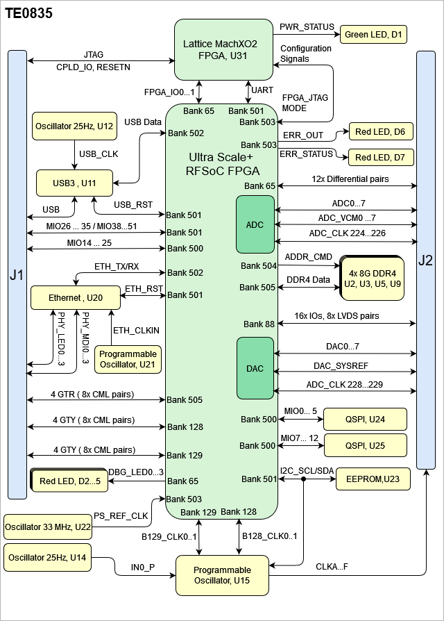
Block Diagram
...
...
...
|
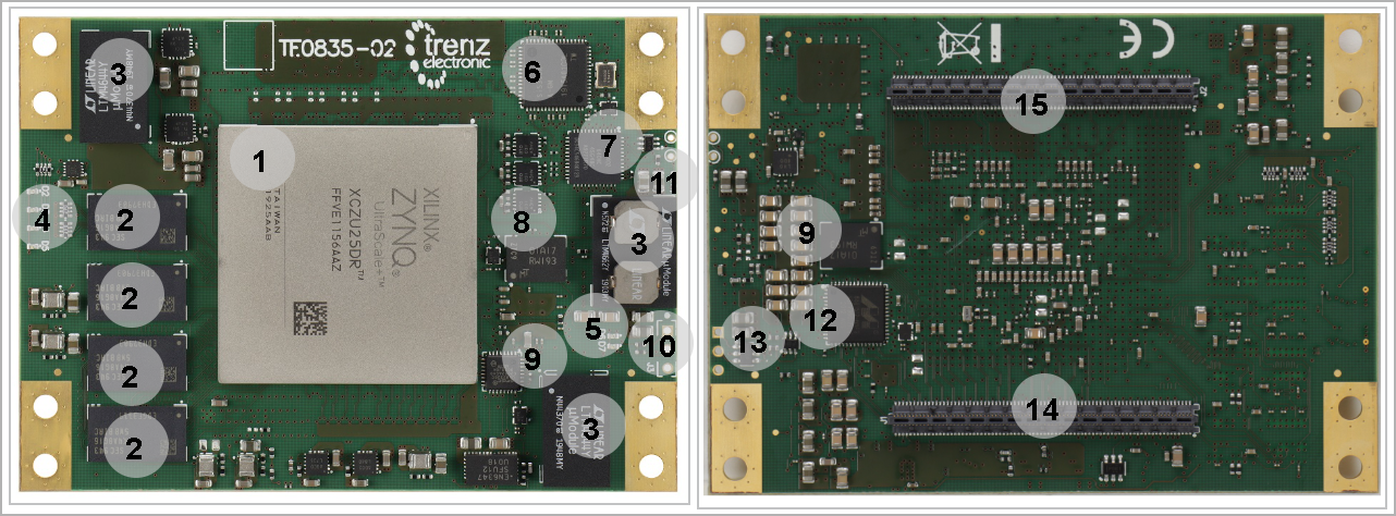
Main Components
| Page properties | ||||
|---|---|---|---|---|
| ||||
Notes :
|
| Scroll Title | |||||||||||||||||
|---|---|---|---|---|---|---|---|---|---|---|---|---|---|---|---|---|---|
| |||||||||||||||||
|
...
|
- Xilinx UltraScale+
...
...
...
...
...
...
...
...
...
...
...
...
| anchor | Table_OV_RST |
|---|---|
| title | Reset process. |
...
Signal
...
RESETN
...
...
...
...
JTAG access to the TExxxx SoM through B2B connector JMX.
...
| anchor | Table_SIP_JTG |
|---|---|
| title | JTAG pins connection |
...
JTAG Signal
...
B2B Connector
...
MIO Pins
...
| hidden | true |
|---|---|
| id | Comments |
you must fill the table below with group of MIOs which are connected to a specific components or peripherals, you do not have to specify pins in B2B, Just mention which B2B is connected to MIOs. The rest is clear in the Schematic.
Example:
...
SPI_CS , SPI_DQ0... SPI_DQ3
SPI_SCK
...
| anchor | Table_OBP_MIOs |
|---|---|
| title | MIOs pins |
...
Test Points
...
...
...
...
...
...
...
...
...
...
...
| Page properties | ||||
|---|---|---|---|---|
| ||||
Notes :
|
| Page properties | ||||
|---|---|---|---|---|
| ||||
Notes : In the on-board peripheral table "chip/Interface" must be linked to the corresponding chapter or subsection |
...
| anchor | Table_OBP |
|---|---|
| title | On board peripherals |
...
...
Notes :
Minimum and Maximum density of quad SPI flash must be mentioned for other assembly options.
...
...
...
...
...
| anchor | Table_OBP_I2C_EEPROM |
|---|---|
| title | I2C address for EEPROM |
...
LEDs
...
| anchor | Table_OBP_RTC |
|---|---|
| title | I2C interface MIOs and pins |
...
| anchor | Table_OBP_I2C_RTC |
|---|---|
| title | I2C Address for RTC |
...
| anchor | Table_OBP_EEP |
|---|---|
| title | I2C EEPROM interface MIOs and pins |
...
...
...
...
...
...
...
| hidden | true |
|---|---|
| id | Comments |
Notes :
...
...
The TE???? SoM has ??? GByte volatile DDR3 SDRAM IC for storing user application code and data.
- Part number:
- Supply voltage:
- Speed:
- NOR Flash
- Temperature:
...
...
...
...
CAN Transceiver
...
| anchor | Table_OBP_CAN |
|---|---|
| title | CAN Tranciever interface MIOs |
...
...
| anchor | Table_OBP_CLK |
|---|---|
| title | Osillators |
...
...
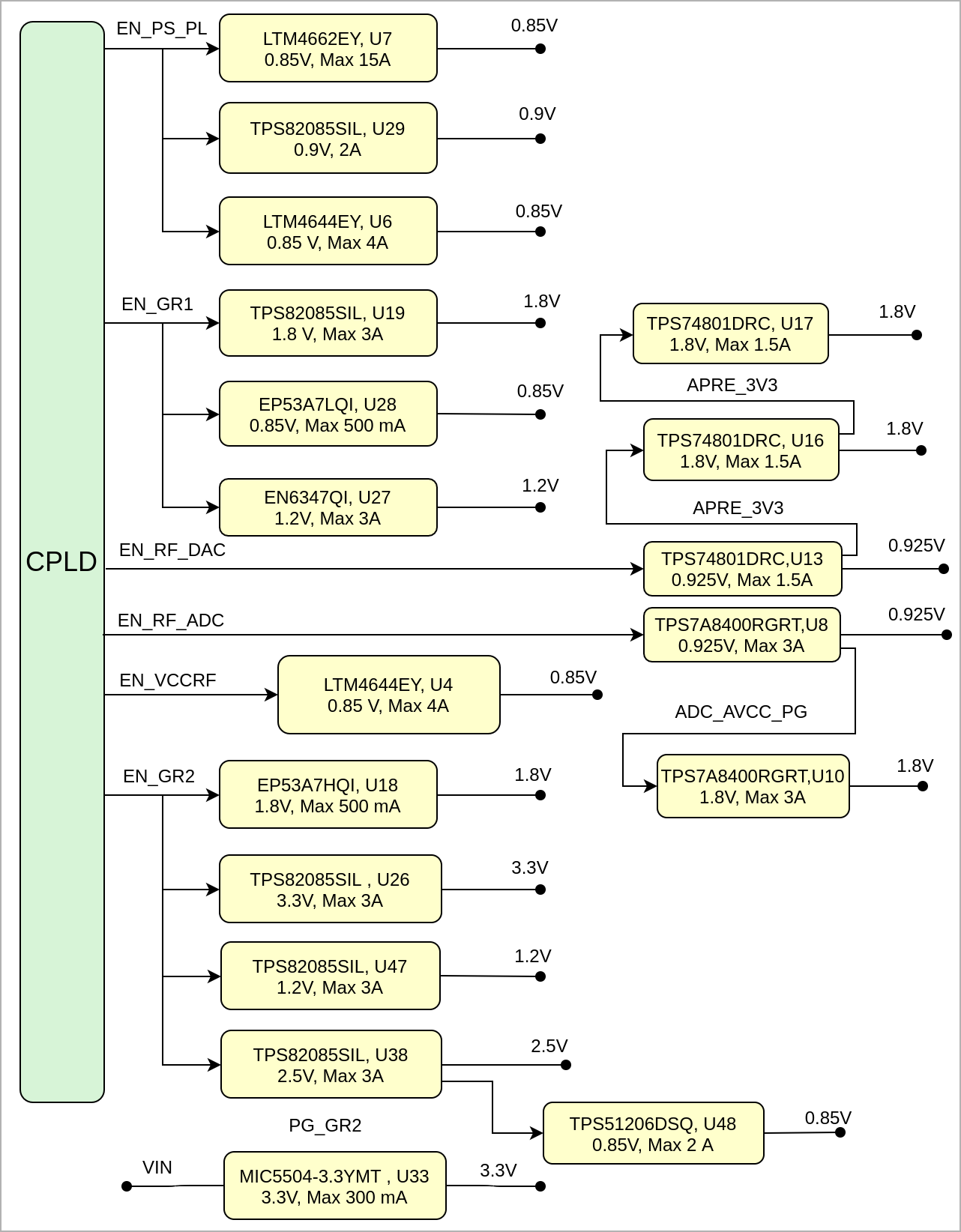
Power Supply
Power supply with minimum current capability of xx A for system startup is recommended.
...
...
...
...
...
|

Power-On Sequence
* TBD - To Be Determined
...
...
...
...
...
...
|
Power
...
...
...
...
...
| Scroll Only |
|---|
|
Voltage Monitor Circuit
...
| anchor | Figure_PWR_VMC |
|---|---|
| title | Voltage Monitor Circuit |
| Scroll Ignore |
|---|
Create DrawIO object here: Attention if you copy from other page, objects are only linked. |
| Scroll Only |
|---|
image link to the generate DrawIO PNG file of this page. This is a workaround until scroll pdf export bug is fixed |
...
...
...
...
...
JM1 Pin
...
B2B Connector
JM2 Pin
...
B2B Connector
JM3 Pin
...
Bank Voltages
...
| anchor | Table_PWR_BV |
|---|---|
| title | Zynq SoC bank voltages. |
...
Bank
...
Voltage
...
...
? x ? modules use two or three Samtec Micro Tiger Eye Connector on the bottom side.
3 x REF-??????? (compatible to ????????), (?? pins, ?? per row)
...
...
...
...
...
...
...
...
...
|
Currently Offered Variants
| Page properties | ||||
|---|---|---|---|---|
| ||||
Set correct link to the shop page overview table of the product on English and German. Example for TE0728: ENG Page: https://shop.trenz-electronic.de/en/Products/Trenz-Electronic/TE07XX-Zynq-SoC/TE0728-Zynq-SoC/ DEU Page: https://shop.trenz-electronic.de/de/Produkte/Trenz-Electronic/TE07XX-Zynq-SoC/TE0728-Zynq-SoC/ For Baseboards or modules, where no overview page is available (and revision number is coded in the direct link) use shop search link, e.g. TE0706: ENG Page: https://shop.trenz-electronic.de/en/search?sSearch=TE0706 DEU Page: https://shop.trenz-electronic.de/de/search?sSearch=TE0706 |
| Scroll Title | ||||||||||||||||||||||
|---|---|---|---|---|---|---|---|---|---|---|---|---|---|---|---|---|---|---|---|---|---|---|
| ||||||||||||||||||||||
| ||||||||||||||||||||||
Revision History
Hardware Revision History
| Page properties | ||||
|---|---|---|---|---|
| ||||
Set correct links to download arrier, e.g. TE0706 REV02: TE0706-02 -> https://shop.trenz-electronic.de/Download/?path=Trenz_Electronic/Modules_and_Module_Carriers/4x5/4x5_Carriers/TE0706/REV02/Documents Note:
|
| Scroll Title | ||||||||
|---|---|---|---|---|---|---|---|---|
| ||||||||
|
...
...
...
...
|
Document Change History
| Page properties | ||||
|---|---|---|---|---|
| ||||
|
| Scroll Title | ||||||||||||||||||||||||||||||||||||||||||||||||
|---|---|---|---|---|---|---|---|---|---|---|---|---|---|---|---|---|---|---|---|---|---|---|---|---|---|---|---|---|---|---|---|---|---|---|---|---|---|---|---|---|---|---|---|---|---|---|---|---|
| ||||||||||||||||||||||||||||||||||||||||||||||||
|
...
| Page info | ||||||||
|---|---|---|---|---|---|---|---|---|
|
...
| Page info | ||||||
|---|---|---|---|---|---|---|
|
...
Overview
Content Tools