Page History
| HTML |
|---|
<!-- tables have all same width (web max 1200px and pdf full page(640px), flexible width or fix width on menu for single column can be used as before) -->
<style>
.wrapped{
  width: 100% !important;
  max-width: 1200px !important;
 }
</style> |
...
| hidden | true |
|---|---|
| id | Comments |
Important General Note:
...
| Scroll pdf ignore | |
|---|---|
Table of Contents
|
...
The module is equipped with 4x 8Gb DDR4 SDRAM Memory, 2x 512Mb SPI Flash Memory, USB2.0, Ethernet Transceiver and 2x Samtec Razor Beam Borard to Board (B2B) Connectors. The system controller CPLD is provided by Lattice MachXO2.
The Zynq UltraScale+ RFSoC family integrates key subsystems for multiband, multi-mode cellular radios and cable infrastructure (DOCSIS) into an SoC platform that contains a feature-rich 64-bitquad-core Arm Cortex-A53 and dual-core Arm Cortex-R5 based processing system.
Refer to http://trenz.org/te0835-info for the current online version of this manual and other available documentation.
| Page properties | ||||
|---|---|---|---|---|
| ||||
Notes :
|
Key Features
| Page properties | ||||
|---|---|---|---|---|
| ||||
Note: Key Features' must be split into 6 main groups for modules and mainboards:
Key Features' must be split into 6 main groups for carrier:
|
| Excerpt |
|---|
|
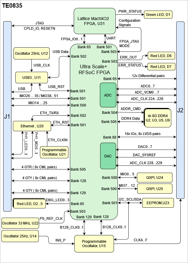
Block Diagram
| Page properties | ||||
|---|---|---|---|---|
| ||||
add drawIO object here.
|
| Scroll Title | ||||||||||||||||||||||||||||||||
|---|---|---|---|---|---|---|---|---|---|---|---|---|---|---|---|---|---|---|---|---|---|---|---|---|---|---|---|---|---|---|---|---|
| ||||||||||||||||||||||||||||||||
|
Main Components
| Page properties | ||||
|---|---|---|---|---|
| ||||
Notes :
|
| Scroll Title | ||||||||||||||||||||||||||||||||
|---|---|---|---|---|---|---|---|---|---|---|---|---|---|---|---|---|---|---|---|---|---|---|---|---|---|---|---|---|---|---|---|---|
| ||||||||||||||||||||||||||||||||
|
- Xilinx UltraScale+ RFSoC, U1
- 8Gb DDR4 SDRAM, U2,U3,U5,U9
- Voltage Regulators, U4,U6,U7
- User Red LEDs, D2...5
- Error/Status Red LEDs, D6...7
- Programmable Glock Generator, U15
- Lattice MachXO2 CPLD, U31
- Dual SPI Flash, U24-U25
- USB2.0 Transceiver, U11
- Pin Header 3x1, J3 (not Soldered)
- Green LED, D1
- Gigabit Ethernet Transceiver, U20
- EEPROM, U23
- B2B Connectors, J1
- B2B Connectors, J2
Initial Delivery State
| Page properties | ||||
|---|---|---|---|---|
| ||||
Notes : Only components like EEPROM, QSPI flash can be initialized by default at manufacture. If there is no components which might have initial data ( possible on carrier) you must keep the table empty |
| Scroll Title | ||||||||||||||||||||||||||||||||||||
|---|---|---|---|---|---|---|---|---|---|---|---|---|---|---|---|---|---|---|---|---|---|---|---|---|---|---|---|---|---|---|---|---|---|---|---|---|
| ||||||||||||||||||||||||||||||||||||
|
Configuration Signals
| Page properties | ||||
|---|---|---|---|---|
| ||||
|
Configuration must be set through CPLD,U31 by setting MODE0...3 signals.
| Scroll Title | ||||||||||||||||||||||||||||||
|---|---|---|---|---|---|---|---|---|---|---|---|---|---|---|---|---|---|---|---|---|---|---|---|---|---|---|---|---|---|---|
| ||||||||||||||||||||||||||||||
|
The reset pin is active low.
| Scroll Title | ||||||||||||||||||||||||||
|---|---|---|---|---|---|---|---|---|---|---|---|---|---|---|---|---|---|---|---|---|---|---|---|---|---|---|
| ||||||||||||||||||||||||||
|
Signals, Interfaces and Pins
Refer to http://trenz.org/te0835-info for the current online version of this manual and other available documentation.
| Page properties | ||||
|---|---|---|---|---|
| ||||
Notes :
|
...
...
...
Key Features' must be split into 6 main groups for modules and mainboards:
- SoC/FPGA
- Package: SFVC784
- Device: ZU2...ZU5*
- Engine: CG, EG, EV*
- Speed: -1LI, -2LE,*, **
- Temperature: I, E,*, **
- RAM/Storage
- Low Power DDR4 on PS
- Data width: 32bit
- Size: def. 2GB*
- Speed:***
- eMMC
- Data width: 8Bit
- size: def. 8GB *
- QSPI boot Flash in dual parallel mode (size depends on assembly version)
- Data width: 8bit
- size: def. 128MB *
- HyperRAM/Flash (optional, default not assembled)
- size:*
- MAC address serial EEPROM with EUI-48™ node identity (Microchip 24AA025E48)
- Low Power DDR4 on PS
- On Board
- Lattice LCMXO2
- PLL SI5338
- Gigabit Ethernet transceiver PHY (Marvell Alaska 88E1512)
- Hi-speed USB2 ULPI transceiver with full OTG support (Microchip USB3320C)
- Interface
- 132 x HP PL I/Os (3 banks)
- ETH
- USB
- 4 GTR (for USB3, Sata, PCIe, DP)
- MIO for UART
- MIO for SD
- MIO for PJTAG
- JTAG
- Ctrl
- Power
- 3.3V-5V Main Input
- 3.3V Controller Input
- Variable Bank IO Power Input
- Dimension
- 4 cm x 5 cm
- Notes
- * depends on assembly version
- ** also non low power assembly options possible
- *** depends on used U+ Zynq and DDR4 combination
Key Features' must be split into 6 main groups for carrier:
- Modules
- TE0808, TE807, TE0803,...
- RAM/Storage
- E.g. SDRAM, SPI
- On Board
- E.g. CPLD, PLL
- Interface
- E.g. ETH, USB, B2B, Display port
- Power
- E.g. Input supply voltage
- Dimension
- SoC/FPGA
- Xilinx UltraScale+ RFSoC (XCZU25DR-1FFVE1156E)
- Package: E1156
- Speed: -1 (slowest)
- Temperature: Extended (0 to +100 °C)
- Xilinx UltraScale+ RFSoC (XCZU25DR-1FFVE1156E)
- RAM/Storage
- 4x 8Gb DDR4
- 2x 512Mb SPI Flash
- 2k I2C EEPROM
- On Board
- Lattice MachXO2 CPLD
- Programmable Clock Generator
- 3x Oscillators
- Interface
- 2x Samtec ST5 (2x80 pol) Board to Board Connectors
- Power
- 5V Input Supply Voltage
- Dimension
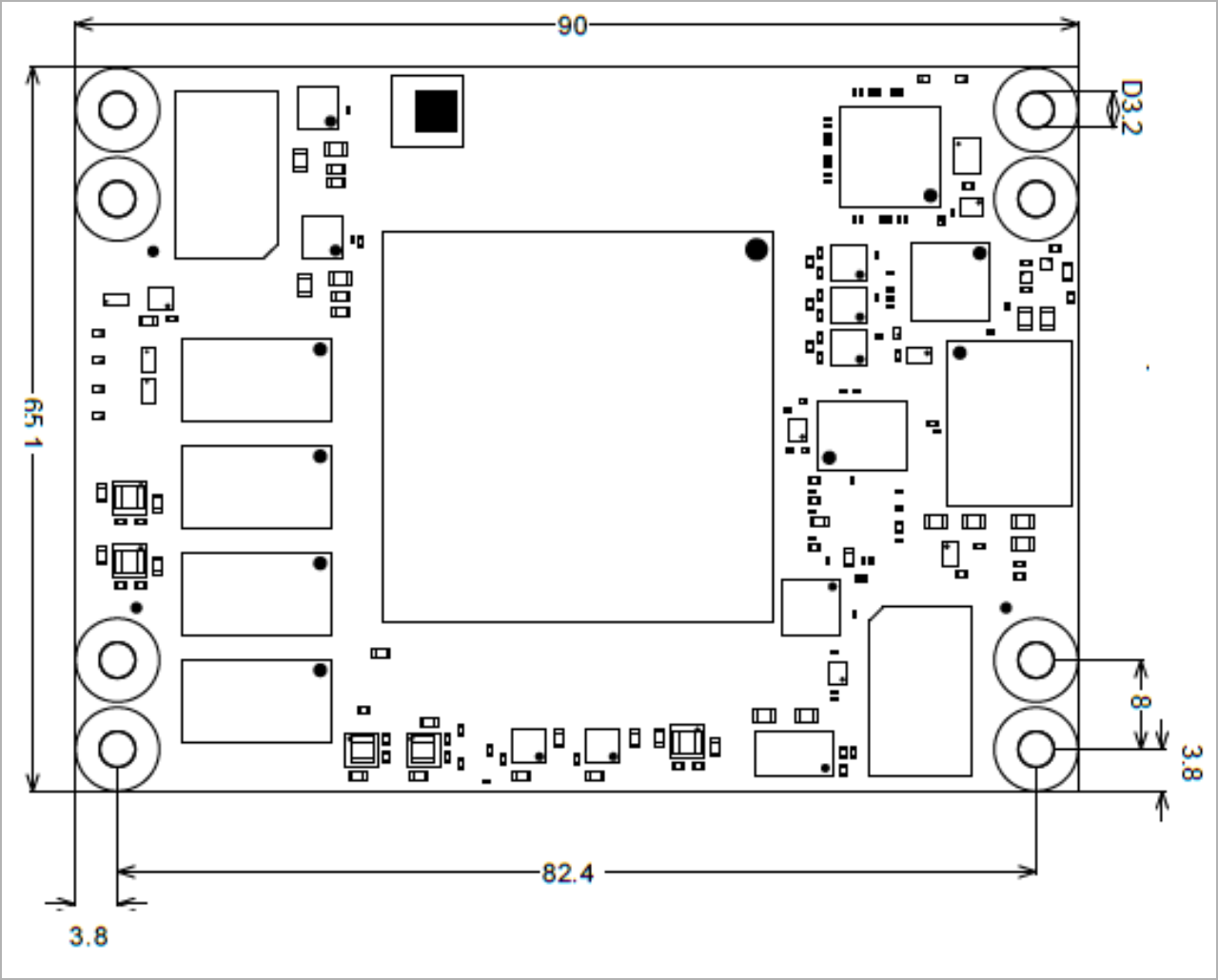
- 90 x 65 mm
Block Diagram
...
| hidden | true |
|---|---|
| id | Comments |
add drawIO object here.
| Note |
|---|
For more information regarding how to draw a diagram, Please refer to "Diagram Drawing Guidline" . |
...
| anchor | Figure_OV_BD |
|---|---|
| title | TE0835 block diagram |
...
| Scroll Only |
|---|
|
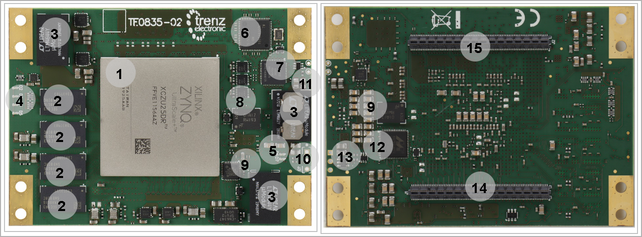
Main Components
...
| hidden | true |
|---|---|
| id | Comments |
Notes :
- Picture of the PCB (top and bottom side) with labels of important components
- Add List below
| Note |
|---|
For more information regarding how to add board photoes, Please refer to "Diagram Drawing Guidline" . |
...
| anchor | Figure_OV_MC |
|---|---|
| title | TE0835 main components |
...
| Scroll Only |
|---|
|
- Xilinx UltraScale+ RFSoC XCZU25DR, U1
- 8Gb DDR4 SDRAM, U2,U3,U5,U9
- Voltage Regulators, U4,U6,U7
- Programmable Glock Generator, U15
- Lattice MachXO2 CPLD, U31
- Dual SPI Flash, U24-U25
- USB2.0 Transceiver, U11
- Pin Header 3x1, J3 (not Soldered)
- Gigabit Ethernet Transceiver, U20
- EEPROM, U23
- B2B Connector, J2
- B2B Connector, J1
Initial Delivery State
| Page properties | ||||
|---|---|---|---|---|
| ||||
Notes : Only components like EEPROM, QSPI flash can be initialized by default at manufacture. If there is no components which might have initial data ( possible on carrier) you must keep the table empty |
...
| anchor | Table_OV_IDS |
|---|---|
| title | Initial delivery state of programmable devices on the module |
...
Storage device name
...
Content
...
Notes
...
2x SPI Flash
...
...
- Overview of Boot Mode, Reset, Enables.
...
...
...
...
...
MODE[0:3]
...
0000
...
PS_JTAG
...
...
| anchor | Table_OV_RST |
|---|---|
| title | Reset process. |
...
Signal
...
RESETN
...
...
...
- SD
- USB
- ETH
- FMC
- ...
...
- JTAG
- UART
- I2C
- MGT
- ...
Board to Board (B2B) I/Os
...
...
...
...
JTAG access to the TE0835 is through B2B connector JM1.
...
| anchor | Table_SIP_JTG |
|---|---|
| title | JTAG pins connection |
...
JTAG Signal
...
B2B Connector
...
J1-22
MIO Pins
...
| hidden | true |
|---|---|
| id | Comments |
you must fill the table below with group of MIOs which are connected to a specific components or peripherals, you do not have to specify pins in B2B, Just mention which B2B is connected to MIOs. The rest is clear in the Schematic.
Example:
...
SPI_CS , SPI_DQ0... SPI_DQ3
SPI_SCK
...
...
...
...
UART_TX, UART_RX
...
...
...
...
Test Points
...
| hidden | true |
|---|---|
| id | Comments |
you must fill the table below with group of Test Point which are indicated as TP in a schematic. If there is no Test Point remarked in the schematic, delet the Test Point section.
Example:
...
| anchor | Table_SIP_TPs |
|---|---|
| title | Test Points Information |
...
B2B, J1
CPLD, U31
...
B2B, J1
CPLD, U31
...
B2B, J1
CPLD, U31
...
B2B, J1
CPLD, U31
...
B2B, J1
CPLD, U31
...
IO_L1P_AD15P_88,
O_L4N_AD12N_88
...
EEPROM,U23
FPGA Bank 501, U1
...
| Page properties | ||||
|---|---|---|---|---|
| ||||
Notes :
|
...
| hidden | true |
|---|---|
| id | Comments |
Notes :
...
...
...
...
Quad SPI Flash Memory
| Page properties | ||||
|---|---|---|---|---|
| ||||
Notes : Minimum and Maximum density of quad SPI flash must be mentioned for other assembly options. |
...
| anchor | Table_OBP_SPI |
|---|---|
| title | Quad SPI interface MIOs and pins |
...
...
...
...
...
...
...
...
...
...
...
| anchor | Table_OBP_I2C_EEPROM |
|---|---|
| title | I2C address for EEPROM |
...
...
...
DDR4 SDRAM
| Page properties | ||||
|---|---|---|---|---|
| ||||
Notes : Minimum and Maximum density of DDR3 SDRAM must be mentioned for other assembly options. (pay attention to supported address length for DDR3) |
The TE???? SoM has ??? GByte volatile DDR3 SDRAM IC for storing user application code and data.
- Part number:
- Supply voltage:
- Speed:
- NOR Flash
- Temperature:
Ethernet
...
...
...
CAN Transceiver
...
| anchor | Table_OBP_CAN |
|---|---|
| title | CAN Tranciever interface MIOs |
...
| anchor | Table_OBP_CLK |
|---|---|
| title | Osillators |
...
...
Power Supply
Power supply with minimum current capability of xx A for system startup is recommended.
...
...
...
...
...
|

Power-On Sequence
* TBD - To Be Determined
...
...
...
...
...
...
|
Power
...
...
...
...
...
| Scroll Only |
|---|
|
Voltage Monitor Circuit
...
| anchor | Figure_PWR_VMC |
|---|---|
| title | Voltage Monitor Circuit |
| Scroll Ignore |
|---|
Create DrawIO object here: Attention if you copy from other page, objects are only linked. |
| Scroll Only |
|---|
image link to the generate DrawIO PNG file of this page. This is a workaround until scroll pdf export bug is fixed |
...
...
...
...
...
JM1 Pin
...
B2B Connector
JM2 Pin
...
B2B Connector
JM3 Pin
...
Bank Voltages
...
| anchor | Table_PWR_BV |
|---|---|
| title | Zynq SoC bank voltages. |
...
Bank
...
Voltage
...
...
...
? x ? modules use two or three Samtec Micro Tiger Eye Connector on the bottom side.
3 x REF-??????? (compatible to ????????), (?? pins, ?? per row)
...
...
...
...
...
...
...
...
...
|
Currently Offered Variants
| Page properties | ||||
|---|---|---|---|---|
| ||||
Set correct link to the shop page overview table of the product on English and German. Example for TE0728: ENG Page: https://shop.trenz-electronic.de/en/Products/Trenz-Electronic/TE07XX-Zynq-SoC/TE0728-Zynq-SoC/ DEU Page: https://shop.trenz-electronic.de/de/Produkte/Trenz-Electronic/TE07XX-Zynq-SoC/TE0728-Zynq-SoC/ For Baseboards or modules, where no overview page is available (and revision number is coded in the direct link) use shop search link, e.g. TE0706: ENG Page: https://shop.trenz-electronic.de/en/search?sSearch=TE0706 DEU Page: https://shop.trenz-electronic.de/de/search?sSearch=TE0706 |
| Scroll Title | ||||||||||||||||||||||
|---|---|---|---|---|---|---|---|---|---|---|---|---|---|---|---|---|---|---|---|---|---|---|
| ||||||||||||||||||||||
| ||||||||||||||||||||||
Revision History
Hardware Revision History
| Page properties | ||||
|---|---|---|---|---|
| ||||
Set correct links to download arrier, e.g. TE0706 REV02: TE0706-02 -> https://shop.trenz-electronic.de/Download/?path=Trenz_Electronic/Modules_and_Module_Carriers/4x5/4x5_Carriers/TE0706/REV02/Documents Note:
|
| Scroll Title | ||||||
|---|---|---|---|---|---|---|
| ||||||
|
...
...
...
...
|
Document Change History
| Page properties | ||||
|---|---|---|---|---|
| ||||
|
| Scroll Title | |||||||||||||||||||||||||||||||||||||||
|---|---|---|---|---|---|---|---|---|---|---|---|---|---|---|---|---|---|---|---|---|---|---|---|---|---|---|---|---|---|---|---|---|---|---|---|---|---|---|---|
| |||||||||||||||||||||||||||||||||||||||
|
...
| Page info | ||||||||
|---|---|---|---|---|---|---|---|---|
|
...
| Page info | ||||||
|---|---|---|---|---|---|---|
|
...
change list
Overview
Content Tools