Page History
...
| HTML |
|---|
<!-- tables have all same width (web max 1200px and pdf full page(640px), flexible width or fix width on menu for single column can be used as before) -->
<style>
.wrapped{
  width: 100% !important;
  max-width: 1200px !important;
 }
</style> |
...
| hidden | true |
|---|---|
| id | Comments |
Important General Note:
...
| Scroll pdf ignore | |
|---|---|
Table of Contents
|
Overview
...
...
...
- E.g. SDRAM, SPI
...
- E.g. CPLD, PLL
...
- E.g. ETH, USB, B2B, Display port
...
- E.g. Input supply voltage
...
...
- Lattice MachXO2 CPLD
- Programmable Clock Generator
- 3x Oscillators
...
- 2x Samtec ST5 (2x80 pol) Board to Board Connectors
...
- 5V Input Supply Voltage
...
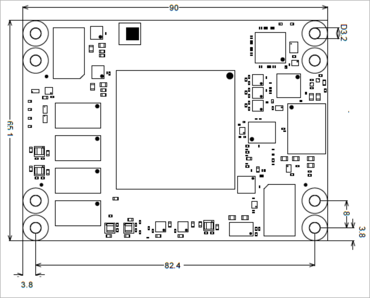
- 90 x 65 mm
Block Diagram
...
| hidden | true |
|---|---|
| id | Comments |
add drawIO object here.
| Note |
|---|
For more information regarding how to draw a diagram, Please refer to "Diagram Drawing Guidline" . |
...
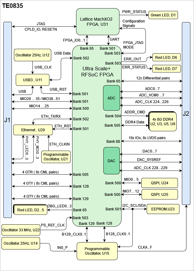
| anchor | Figure_OV_BD |
|---|---|
| title | TE0835 block diagram |
...
| Scroll Only |
|---|
|
...
Notes :
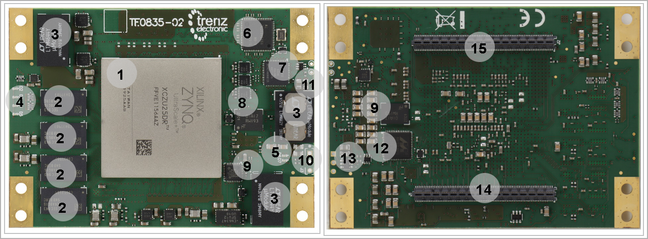
- Picture of the PCB (top and bottom side) with labels of important components
- Add List below
...
...
...
...
...
...
2x SPI Flash
...
Configuration Signals
...
- Xilinx UltraScale+ RFSoC XCZU25DR, U1
- 8Gb DDR4 SDRAM, U2,U3,U5,U9
- Voltage Regulators, U4,U6,U7
- Programmable Glock Generator, U15
- Lattice MachXO2 CPLD, U31
- Dual SPI Flash, U24-U25
- USB2.0 Transceiver, U11
- Pin Header 3x1, J3 (not Soldered)
- Gigabit Ethernet Transceiver, U20
- EEPROM, U23
- B2B Connector, J2
- B2B Connector, J1
Initial Delivery State
| Page properties | ||||
|---|---|---|---|---|
| ||||
Notes : Only components like EEPROM, QSPI flash can be initialized by default at manufacture. If there is no components which might have initial data ( possible on carrier) you must keep the table empty |
...
| anchor | Table_OV_IDS |
|---|---|
| title | Initial delivery state of programmable devices on the module |
...
Storage device name
...
Content
...
Notes
|
Main Components
| Page properties | ||||
|---|---|---|---|---|
| ||||
Notes :
|
| Scroll Title | ||||||||||||||||||||||||||||||||
|---|---|---|---|---|---|---|---|---|---|---|---|---|---|---|---|---|---|---|---|---|---|---|---|---|---|---|---|---|---|---|---|---|
| ||||||||||||||||||||||||||||||||
|
- Xilinx UltraScale+ RFSoC, U1
- 8Gb DDR4 SDRAM, U2,U3,U5,U9
- Voltage Regulators, U4,U6,U7
- User Red LEDs, D2...5
- Error/Status Red LEDs, D6...7
- Programmable Glock Generator, U15
- Lattice MachXO2 CPLD, U31
- Dual SPI Flash, U24-U25
- USB2.0 Transceiver, U11
- Pin Header 3x1, J3 (not Soldered)
- Green LED, D1
- Gigabit Ethernet Transceiver, U20
- EEPROM, U23
- B2B Connectors, J1
- B2B Connectors, J2
Initial Delivery State
...
- Overview of Boot Mode, Reset, Enables.
...
...
...
...
MODE[0:3]
...
0000
...
PS_JTAG
...
...
...
...
...
...
...
...
...
System Controller CPLD
The System Controller CPLD (U31) is provided by Lattice Semiconductor LCMXO2-460HC. The SC-CPLD is the central system management unit where essential control signals are logically linked by the implemented logic in CPLD firmware, which generates output signals to control the system, the on-board peripherals and the interfaces. Interfaces like JTAG / UART and I2C between the on-board peripherals and the attached module are by-passed, forwarded and controlled by the System Controller CPLD.
...
...
...
...
...
...
...
...
|

Power-On Sequence
| Scroll Title | |||||||||||||||||
|---|---|---|---|---|---|---|---|---|---|---|---|---|---|---|---|---|---|
| |||||||||||||||||
|
...
|
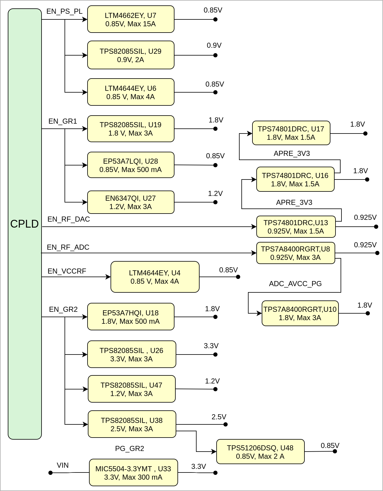
Power Rails
| Scroll Title | |||||||||||||||||||
|---|---|---|---|---|---|---|---|---|---|---|---|---|---|---|---|---|---|---|---|
| |||||||||||||||||||
|
B2B Connector
...
B2B Connector
...
...
...
...
...
...
...
...
...
...
The TE0835 has two Samtec Razor Beam on the bottom side.
...
...
...
...
...
...
...
...
...
see USB3320 Datasheet
...
|
Currently Offered Variants
| Page properties | ||||
|---|---|---|---|---|
| ||||
Set correct link to the shop page overview table of the product on English and German. Example for TE0728: ENG Page: https://shop.trenz-electronic.de/en/Products/Trenz-Electronic/TE07XX-Zynq-SoC/TE0728-Zynq-SoC/ DEU Page: https://shop.trenz-electronic.de/de/Produkte/Trenz-Electronic/TE07XX-Zynq-SoC/TE0728-Zynq-SoC/ For Baseboards or modules, where no overview page is available (and revision number is coded in the direct link) use shop search link, e.g. TE0706: ENG Page: https://shop.trenz-electronic.de/en/search?sSearch=TE0706 DEU Page: https://shop.trenz-electronic.de/de/search?sSearch=TE0706 |
| Scroll Title | ||||||||||||||||||||||
|---|---|---|---|---|---|---|---|---|---|---|---|---|---|---|---|---|---|---|---|---|---|---|
| ||||||||||||||||||||||
| ||||||||||||||||||||||
Revision History
Hardware Revision History
| Page properties | ||||
|---|---|---|---|---|
| ||||
Set correct links to download arrier, e.g. TE0706 REV02: TE0706-02 -> https://shop.trenz-electronic.de/Download/?path=Trenz_Electronic/Modules_and_Module_Carriers/4x5/4x5_Carriers/TE0706/REV02/Documents Note:
|
| Scroll Title | ||||||||
|---|---|---|---|---|---|---|---|---|
| ||||||||
|
...
...
|
Document Change History
| Page properties | ||||
|---|---|---|---|---|
| ||||
|
| Scroll Title | |||||||||||||||||||||||||||||||||||||||||||||||||||
|---|---|---|---|---|---|---|---|---|---|---|---|---|---|---|---|---|---|---|---|---|---|---|---|---|---|---|---|---|---|---|---|---|---|---|---|---|---|---|---|---|---|---|---|---|---|---|---|---|---|---|---|
| |||||||||||||||||||||||||||||||||||||||||||||||||||
|
...
Overview
Content Tools