Modified TE0703 with TEM0007
Overview
TEM0007 module is a Microchip Polarfire SoC module. For more information about this module refer to TEM0007 TRM
Hardware overview
Required Hardware
| Hardware | Quantity | Note |
|---|---|---|
| TEM0007 | 1 | Microchip Polarfire SoC Module |
| Modified TE0703 | 1 | Carrier board Modified TE0703:
|
| TE0790 | 1 | Universal USB2.0 to JTAG/UART |
| Mini USB Cable | 2 | |
| RJ45 Ethernet Cable | 1 | |
| USB Stick | 1 | |
| Heatsink | 1 |
Modification TE0703
It is necessary to modify the TE0703 carrier board for using TEM0007 module. In the following will be in detail discussed the modification of TE0703 carrier board.
SD Jumper
Jumper J11 must be set to 3.3V.
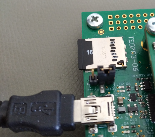
Set SD card voltage
XMOD UART(HSS)
It is recommended to use second UARD interface to see the HSS console. The UART pins mus be connected to XMOD module ( TE0790 ). The TE0790 is a universal USB2.0 to JTAG/UART converter.For more infomation about this module refer to TE0790 TRM
For this purpose see the following table:| TE0703 Pin | Schematic label | TE0790 Pin | Schematic label | Description |
|---|---|---|---|---|
J2A-Pin A31 (TXD) | X17 | J2-Pin 3 (RXD) | A | |
J2A-Pin A30 (RXD) | X16 | J2-Pin 5 (TXD) | B | |
| J2A-Pin A32 (GND) | --- | J2-Pin 1 | --- |
JTAG FTDI
Driver of FTDI chip must be reprogrammed. It must be mached with microchip FPGAs.
USB OTG
The following components of the TE0703 must be changed , if these don't exist on the board or other component is soldered :
| Component | Designator | Value | Description |
|---|---|---|---|
USB connector | J12 | --- | Micro USB2 B 90° |
| Choke | L4 | --- | SMD Line Filter WE-CNSW-HF |
| Resistor | R5 | 1k 1% | |
| Capacitor | C5 | 4.7uf 25V | X7R AEC-Q200 |
| Capacitor | C27 | 4.7uf 25V | X7R AEC-Q200 |
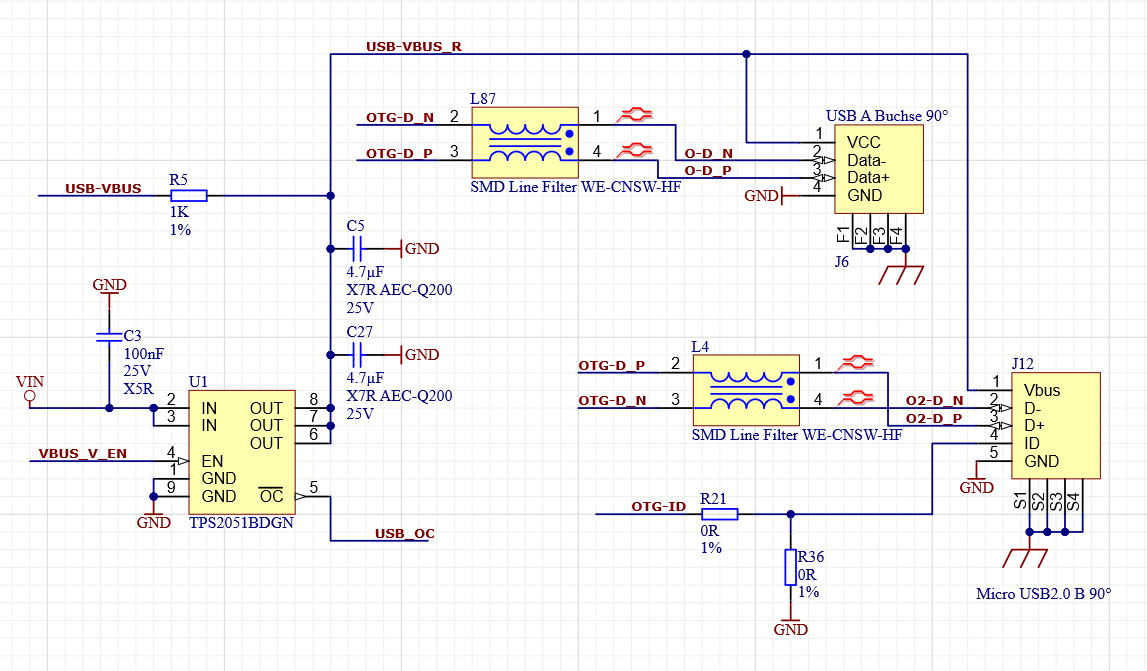
USB schematic
Reset Button
It is installed a power reset button. But to have a soft reset button optional can be connected a push button with a pulled up resistor as shown:
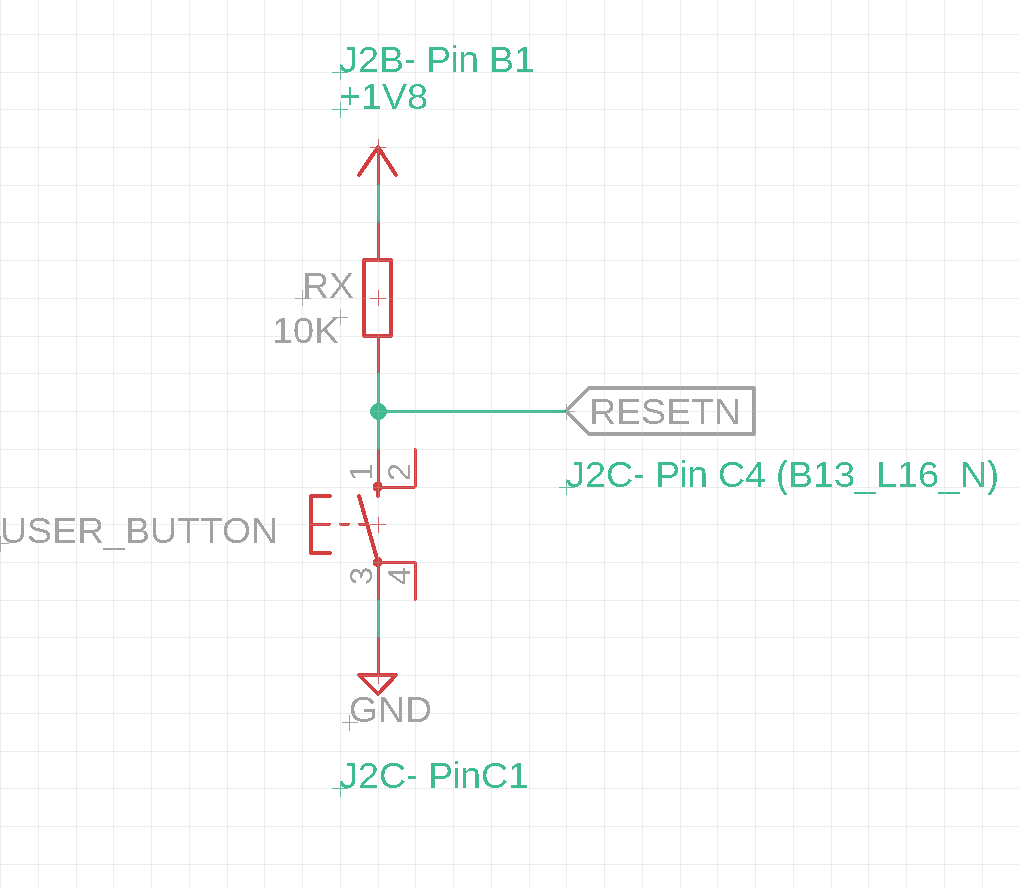
Reset Schematic
| Pin | TE0703 Schematic label | Description |
|---|---|---|
| 3.3V | J2B- Pin B1 | VG96 female header vertical |
| GND | J2C-Pin C1 | VG96 female header vertical |
| RESETN | J2C-Pin C4 | VG96 female header vertical |
Power supply
| Supply voltage | Current | Designator | Description |
|---|---|---|---|
| 5V | 2A* | J13 on the carrier board |
*Current is dependent on design and the used heatsink. This value is recommend value.
DIP Switches
In this case S2 dip switches can be use for JTAG adjustment only and it will not be used to select boot mode, because TEM0007 supports only SD card boot mode.
| S2-1 | S2-2 | S2-3 | S2-4 | Description |
|---|---|---|---|---|
| CM1 | CM0 | JTAGEN | MIO0 |
| S2-2 | S2-3 | CM0 | JTAGEN | Description |
|---|---|---|---|---|
| OFF | OFF | 1 | 1 | Access to TE0703 CPLD |
| OFF | ON | 1 | 0 | Access to CPLD of TEM0007 |
| ON | OFF | 0 | 1 | Access to TE0703 CPLD |
| ON | ON | 0 | 0 | Access to FPGA of TEM0007 |
Jumpers
| Jumper | related net | Allowed to set on | Description |
|---|---|---|---|
| J11 | VCCA pin of voltage level shifter chip ( TXS02612RTWR ) | 3.3V | If this jumper set to 1.8V , SD card will not work. |
J5 | VCCIOA | --- | Not necessary |
J8 | VCCIOB | 1.8V / 3.3V | This jumper can be set to 1.8V or 3.3V. |
J9 | VCCIOC | --- | Not necessary |
| J10 | VCCIOD | Only 1.8V | Set to 1.8V |
Resets
There are one reset push button on the board. Second reset button can be added on the board as optional reset.
| Signal | Push button | FPGA Pin | Schematic label | New design label | Connected to | Access on the carrier board via | Description |
|---|---|---|---|---|---|---|---|
| RESET (RESIN) | S1 | H7 | DEVRST_N | --- | TPS3106K33DBV chip RSTVDD Pin / CPLD of TEM0007 via B2B connector (SC_RESET / MR_n) | S1 | This reset signal does not exist in Libero design. This reset signal resets FPGA via CPLD Firmware of TEM0007 module. By pushing S1 (RESIN) push button will set DEVRST_N to low. |
| RESETN | User button | H13 | B1_GPIO185_N | RESETN | JM2-Pin 73 | JB2-pin 74 / J2C-C4 | User button does not exist on the carrier board. User button should be soldered by the user himself. (Optional) This button should be pulled up via a 10k resistor. |
Boot mode
SD Card
This module supports SD card boot mode. There is no dip switch to select boot mode.
JTAG
-TODO
Peripheral interfaces
JTAG
JTAG geht über MiniUSB und FTDI. Kein extra Programmer nötig
UART
There is two UART interfaces.
| UART | FPGA Pin | Schematic label | New design label | Connected to | Access on the carrier board via | Interface for | Baud rate | Description |
|---|---|---|---|---|---|---|---|---|
| UART0 | C2 (TXD) | UART_CON_TX | MMUART_0_TXD | JM1-Pin 99 | JB1-Pin 100 / J2A-Pin 31 (TXD) | HSS (Hardware System Service) | 115200 | There is no connector on the TE0703 carrier board PCB REV06. In this case user should connect these pins to USB to JTAG/UART converter same as TE0790. (Crosstalk) |
| D3 (RXD) | UART_CON_RX | MMUART_0_RXD | JM1-Pin 97 | JB1-Pin 98 / J2A-Pin 30 (RXD) | ||||
| UART1 | H5 (TXD) | UART_TX | MMUART_1_TXD | JM1-Pin 85 | JB1-Pin 86 / | Linux console / Bare metal interface | 115200 | |
| H2 (RXD) | UART_RX | MMUART_1_RXD | JM1-Pin 92 | JB1-Pin 91 / J4 Mini USB connector |
I2C
| I2C | FPGA Pin | Schematic label | New design label | Connected to | Access on the carrier board via | Description |
|---|---|---|---|---|---|---|
| I2C0 | A3 (SCL) | I2C_CON_SCL | I2C_0_SCL | JM1-Pin 95 | JB1-Pin 96 (SCL) | |
| E3 (SDA) | I2C_CON_SDA | I2C_0_SDA | JM1-Pin 93 | JB1-Pin 94 (SDA) | ||
| I2C1 | C1 (SCL) | I2C_SCL | I2C_1_SCL | EEPROM chip U10 SCL pin | No Access | |
| B1 (SDA) | I2C_SDA | I2C_1_SDA | EEPROM chip U10 SDA pin | No Access | ||
| CORE_I2C | B8 (SCL) | B1_GPIO175_N | USER_I2C0_SCL | JM1-Pin 62 | JB1-Pin 61 | This additional i2c interface in generated via COREI2C. (Old names CORE_I2C_C0_INT , COREI2C_C0_SCL and COREI2C_C0_SDA) |
| A8 (SDA) | B1_GPIO175_P | USER_I2C0_SDA | JM1-Pin 60 | JB1-Pin 59 | ||
| RPI_I2C | F10 (SCL) | B1_GPIO180_N | USER_I2C1_SCL | JM2-Pin 85 | JB2-Pin 86 | This additional i2c interface in generated via COREI2C. (Old names RPi_ID_I2C_IRQ, RPi_ID_SC and RPi_ID_SD) |
| B9 (SDA) | B1_GPIO179_N | USER_I2C1_SDA | JM1-Pin 68 | JB1-Pin 67 |
Ethernet
| Signal | FPGA Pin | Schematic label | New design label | Connected to | Access on the carrier board via | Description |
|---|---|---|---|---|---|---|
| MAC_0_MDIO | J3 | ETH_MDIO | MAC_0_MDIO | Ethernet Phy Chip (Marvell 88E1512-A0-NNP2I000) Pin 8 | No Access | |
| MAC_0_MDO | H6 | ETH_MDO | MAC_0_MDO | Ethernet Phy Chip (Marvell 88E1512-A0-NNP2I000) Pin 7 | No Access |
UART
There is two UART interfaces.
| UART | FPGA Pin | Schematic label | New design label | Connected to | Access on the carrier board via | Interface for | Baud rate | Description |
|---|---|---|---|---|---|---|---|---|
| UART0 | C2 (TXD) | UART_CON_TX | MMUART_0_TXD | JM1-Pin 99 | JB1-Pin 100 / J2A-Pin 31 (TXD) | HSS (Hardware System Service) | 115200 | There is no connector on the TE0703 carrier board PCB REV06. In this case user should connect these pins to USB to JTAG/UART converter same as TE0790. (Crosstalk) |
| D3 (RXD) | UART_CON_RX | MMUART_0_RXD | JM1-Pin 97 | JB1-Pin 98 / J2A-Pin 30 (RXD) | ||||
| UART1 | H5 (TXD) | UART_TX | MMUART_1_TXD | JM1-Pin 85 | JB1-Pin 86 / | Linux console / Bare metal interface | 115200 | |
| H2 (RXD) | UART_RX | MMUART_1_RXD | JM1-Pin 92 | JB1-Pin 91 / J4 Mini USB connector | ||||
| COREUARTapb | A7 (TXD) | B1_GPIO173_P | COREUART_TX | JM1-Pin 65 | JB1-Pin 66 | Additional UART interface | Depends on system clock frequency. Baud_rate = clk/(Baudval+1)*16 and Baudval = (clk/(1+Baudrate)) - 1 | This UART interface works via COREUARTapb in Libero. |
| H15 (RXD) | B1_GPIO7_N | COREUART_RX | JM2-Pin 66 | JB2-Pin 65 | ||||
| mBUS_UART | B20 (TXD) | B1_GPIO19_P | USER_UART_TX | JM2-Pin 46 | JB2-Pin 45 | Additional UART interface | 115200 | Old names mBUS_UART_TX, mBUS_UART_RX and mBUS_INT |
| A21 (RXD) | B1_GPIO20_N | USER_UART_RX | JM2-Pin 32 | JB2-Pin 31 | ||||
| A20 (INT) | B1_GPIO20_P | USER_UART_INT | JM2-Pin 34 | JB2-Pin 33 |
LED
USB
GPIOs
| GPIO | FPGA Pin | Schematic label | New design label | Connected to | Access on the carrier board via | Description |
|---|---|---|---|---|---|---|
| GPIO_1_16 | E5 | ETH_RST | ETH_PHY_RESET | ETH_RST | No Access | Phy chip reset pin (Marvell 88E1512-A0-NNP2I000). Necessary for reset pin of ethernet phy chip |
| GPIO_1_17 | E4 | OTG-RST | USB_PHY_RESET | OTG-RST | No Access | USB phy chip reset pin (Microchip USB3320-EZK). Necessary for reset pin of usb phy chip |
| GPIO_1_18 | B2 | --- | Not used | --- | No Access | |
| GPIO_1_19 | A2 | --- | Not used | --- | No Access | |
| GPIO_1_20 | B3 | GPIO1 | GPIO_1_20 | B2B JM1-Pin 91 | B2B JB1-Pin 92 | |
| GPIO_1_23 | D4 | GPIO0 | GPIO_1_23 | B2B JM1-Pin 87 | B2B JB1-Pin 88 | |
| GPIO_2_0 | U12 | B0_HSIO94_P | Not used | --- | No Access | |
| GPIO_2_1 | T13 | B0_HSIO95_N | Not used | --- | No Access | |
| GPIO_2_6 | R12 | B0_HSIO95_P | Not used | --- | No Access | |
| RPi_GPIO12 | D9 | GPIO174_P | GPIO_2_2 | JM1-Pin 69 | JB1-Pin 70 | |
| RPi_GPIO13 | D6 | GPIO168_N | GPIO_2_3 | JM1-Pin 88 | JB1-Pin 87 | |
| RPi_GPIO16 | C6 | GPIO171_P | GPIO_2_4 | JM1-Pin 83 | JB1-Pin 84 | |
| RPi_GPIO17 | H17 | GPIO8_N | GPIO_2_5 | JM2-Pin 62 | JB2-Pin 61 | |
| RPi_GPIO19 | B5 | GPIO170_N | GPIO_2_7 | JM1-Pin 70 | JB1-Pin 69 | |
| RPi_GPIO20 | C5 | GPIO170_P | GPIO_2_8 | JM1-Pin 72 | JB1-Pin 71 | |
| RPi_GPIO21 | C4 | GPIO169_P | GPIO_2_9 | JM1-Pin 77 | JB1-Pin 78 | |
| RPi_GPIO22 | F11 | GPIO181_N | GPIO_2_10 | JM2-Pin 65 | JB2-Pin 66 | |
| RPi_GPIO23 | F16 | GPIO11_N | GPIO_2_11 | JM2-Pin 41 | JB2-Pin 42 | |
| RPi_GPIO24 | D14 | GPIO2_N | GPIO_2_12 | JM1-Pin 46 | JB1-Pin 45 | |
| RPi_GPIO25 | E14 | GPIO9_N | GPIO_2_13 | JM2-Pin 57 | JB2-Pin 58 | |
| RPi_GPIO26 | B4 | GPIO169_N | GPIO_2_14 | JM1-Pin 75 | JB1-Pin 76 | |
| RPi_GPIO27 | G17 | GPIO8_P | GPIO_2_15 | JM2-Pin 64 | JB2-Pin 63 |
User IOs
| Input | FPGA Pin | Schematic label | New design label | Connected to | Access on the carrier board via | Description |
|---|---|---|---|---|---|---|
| SW1 | V19 | B0_HSIO72_N | USER_IN0 | JM3-Pin 42 | JB3-Pin 41 | |
| SW2 | U18 | B0_HSIO74_N | --- | --- | No Access | |
| SW3 | W19 | B0_HSIO79_P | --- | --- | No Access | |
| SW4 | H13 | B1_GPIO185_N | RESETN | JM2-Pin 73 | JB2-Pin 74 | Used as RESETN Pin |
| Output | FPGA Pin | Schematic label | New design label | Connected to | Access on the carrier board via | Description |
|---|---|---|---|---|---|---|
| LED0 | V14 | B0_HSIO90_P | --- | --- | No Access | |
| LED1 | U13 | B0_HSIO93_N | --- | --- | No Access | |
| LED2 | T12 | B0_HSIO94_N | --- | --- | No Access | |
| LED3 | AB19 | B0_HSIO70_P | USER_OUT0 | JM3-Pin 60 | JB3-Pin 59 |
PWM
| Signal | FPGA Pin | Schematic label | New design label | Connected to | Access on the carrier board via | Description |
|---|---|---|---|---|---|---|
| PWM | E11 | B1_GPIO183_N | USER_PWM0 | JM1-Pin 82 | JB1-Pin 81 / J1C-Pin C4 |
Table of contents
Overview
Content Tools