Table of Contents
Overview
The Trenz Electronic TE0706 is a baseboard intended for use with 4x5 SoMs manufactured by the company. Baseboard exposes MIO- and PS/PL-pins of the SoM to accessible connectors and provides a whole range of on-board components for SoMs evaluation and testing.
See page "4x5 cm carriers" for information about the SoMs supported by the TE0706.
Block Diagram
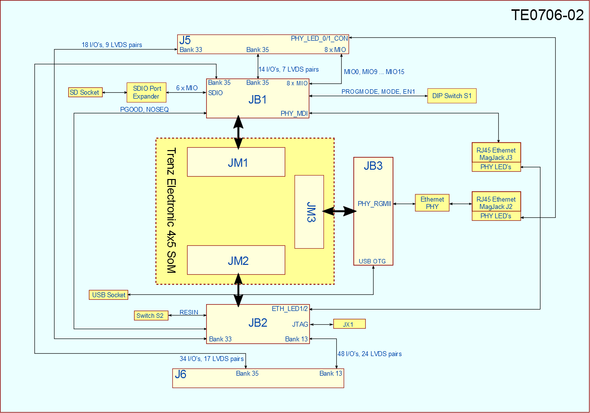
Main Components
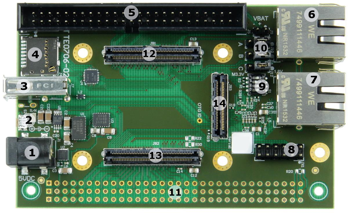
- 5V power connector jack, J1
- Reset switch, S2
- USB type A receptacle, J7
- Micro SD card socket with detect switch, J4
- 50 pin IDC male connector, J5
- 1000Base-T Gigabit RJ45 Ethernet MagJack, J3
- 1000Base-T Gigabit RJ45 Ethernet MagJack, J2
- JTAG Connector, JX1
- User DIP switch block, S1
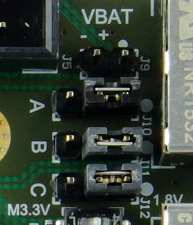
- VCCIO voltage selection jumper block, J10 - J12
- External connector (VG96) placeholder, J6
- Samtec Razor Beam™ LSHM-150 B2B connector, JB1
- Samtec Razor Beam™ LSHM-150 B2B connector, JB2
- Samtec Razor Beam™ LSHM-130 B2B connector, JB3
Key Features
- VG96 backplane connector (mounting holes and solder pads, J6) and 50-pin IDC male connector socket (J5) to access FPGA bank's I/O-pins
- SDIO port expander with voltage-level translation
- Micro SD card socket, routed to B2B-connector JB1
- USB type A connector (OTG mode), routed to B2B-connecor JB3
- 1 x user-push button S2, routed to RESIN-pin on B2B-connector JB2. By default it is configured as system reset button.
- 1 x RJ45 Gigabit Ethernet MagJack J3, PHY_MDI interface routed to B2B-connector JB1.
- 1 x Marvell Alaska 88E1512 Ethernet PHY, routed to B2B-connector JB3 and accessible via RJ45 Gigabit Ethernet MagJack J2
- Barrel jack for 5 V Power Supply input
- 4 A High-Efficiency Power SoC DC-DC Step-Down Converter (Enpirion EN6347) for 3.3 V Power Supply
- Trenz 4x5 Module Socket (3 x Samtec LSHM series connectors)
- JTAG pins on 12-pin header JX1, routed to B2B-connector JB2
- user configurable DIP switch S1 to set System Controller CPLD signals on SoM
- 3 x VCCIO selection jumper J10, J11 and J12 to set SoM s bank voltages
Initial Delivery State
Board is shipped in following configuration:
- VCCIO voltage selection jumpers are all set to 1.8 V.
- S2 switch configured as reset button.
- One VG96 backplane connector is not soldered to the board, but is included in the package as separate component.
Different delivery configurations are available upon request.
Signals, Interfaces and Pins
Board to Board (B2B) I/Os
For detailed information about the B2B pin out, please refer to the Master Pin-out Table.
JTAG Interface
JTAG access to the SoMs Xilinx Zynq chip on the SoM is provided via 12-pin header JX1 and controlled by DIP switch S1-2. JTAG pins are routed to the JB2 and JX1 connectors as follows:
JTAG Signal | B2B Connector | 12-pin header JX1 |
|---|---|---|
| TMS | JB2-94 | 12 |
| TDO | JB2-98 | 8 |
| TDI | JB2-96 | 10 |
| TCK | JB2-100 | 4 |
Micro SD Card Socket
Micro SD Card socket is not directly wired to the B2B connector pins, but through a Texas Instruments TXS02612 SDIO port expander, which is needed for voltage translation due to the different voltage levels of the Micro SD Card and MIO bank 501 of the Xilinx Zynq 7000 chip. The Micro SD Card has 3.3 V signal voltage-level, but the MIO Bank 501 on the Xilinx Zynq 7000 chip is set to 1.8 V.
Ethernet
The TE0706-02 is equipped with a Marvell Alaska 88E1512 Gigabit Ethernet PHY (U6) connected to the B2B connector JB3. The I/O Voltage is fixed at 1.8V. The reference clock input of the PHY is supplied by on-board 25MHz oscillator (U7).
PHY (U6) interface connections:
| PHY | B2B-pin | Notes |
|---|---|---|
| MDC/MDIO | JB3-49, JB3-51 | - |
| LED0 | - | Connected to Ethernet jack J2 LED0 (green). |
| LED1 | - | Connected to Ethernet jack J2 LED1 (green). |
| INT | JB3-33 | - |
| CONFIG | JB3-60 | - |
| RESET | JB3-53 | - |
| RGMII | JB3-37 - JB-44, JB3-47, JB3-57 - JB-59 | 12 pins. |
| SGMII | - | Not connected. |
| MDI | - | Connected to Gigabit-Ethernet MagJack J2. |
RJ45 Gigabit Ethernet MagJack J3
The TE0706-02 carrier board is also equipped with a second Gigabit-Ethernet MagJack J3, which is connected via MDI to the B2B connector JB1.
There is usually a corresponding Gigabit Ethernet PHY on 4x5 SoMs (e.g. TE0715 or TE0720), which can be used in conjunction with the baseboard MagJack J3.
USB Interface
TE0706-02 board has one physical USB type A socket J7 routed to B2B connector JB3. The corresponding USB-transceiver on 4x5 SoMs varies in order of the used SoM model.
There is also the option to equip a micro USB 2.0 type B receptacle socket (J8) to the board as alternative.
Note: Pin OTG-ID is only assigned to USB 2.0 type B socket.
DIP switch S1
| Switch | Signal Name | ON | OFF | Notes |
|---|---|---|---|---|
| S1-1 | - | - | - | Not connected |
| S1-2 | PROGMODE | JTAG enabled for programing SoM FPGA | JTAG enabled for programing SoM CPLD | - |
| S1-3 | MODE | Drive SoM SC CPLD pin 'MODE' low | leave SoM SC CPLD pin 'MODE' open | Boot mode configuration, if supported by SoM. (Depends also on SoM SC CPLD firmware). |
| S1-4 | EN1 | Drive SoM SC CPLD pin 'EN1' low | drive SoM SC CPLD pin 'EN1' high | Usually used to enable/disable FPGA core-voltage supply. (Depends also on SoM SC CPLD firmware). Note: Power-on sequence will be intermitted when S1-4 is set to OFF and functionality is supported by SoM. |
Power and Power-On Sequence
Power supply with minimum current capability of 3A for system startup is recommended.
Power Supply
TE0706-02 needs one single power supply with nominal of 5V.
Power Consumption
| Power Input Pin | Max Current |
|---|---|
| VIN | 4A |
Typical power consumption for TE0706-02 in conjunction with different 4x5 SoMs under certain configurations will be determined soon.
Power-On Sequence
It is not allowed to feed any voltage to any external I/O pin before there is no power indication on M3.3VOUT pins. Presence of 3.3V on B2B JB2 connector pins 9 and 11 indicates that module is properly powered up and ready.
If VCCIOA or VCCIOC will be powered through the dedicated pins of external connector J6, then corresponding VCCIO jumpers J10 and J12 should be removed.
VCCIO voltage selection jumpers J10, J11 and J12
Refer to the 4x5 Module Integration Guide for VCCIO voltage options.
Baseboard supply voltage | Baseboard B2B connector pins | Standard assignment of PL I/O bank supply voltages on TE 4x5 module's B2B connectors |
|---|---|---|
| VCCIOA | JB1-10, JB1-12 | VCCIOA (JM1-9, JM1-11) |
| VCCIOB | JB2-6 | VCCIOC (JM2-5) |
| VCCIOC | JB2-8, JB2-10 | VCCIOD (JM2-7, JM2-9) |
| Fixed 1.8V | JB2-2, JB2-4 | VCCIOB (JM2-1, JM2-3) |
Note: The corresponding PL I/O bank supply voltages of the 4x5 SoM to the selectable baseboard voltages VCCIOA, VCCIOB and VCCIOC are depending on the mounted 4x5 SoM and varying in order of the used model.
Refer to the SoMs schematic for information about the specific pin assignments on module's B2B-connectors regarding the PL I/O bank supply voltages and to the 4x5 Module integration Guide for VCCIO voltage options.
Following table describes how baseboard supply voltages VCCIOA, VCCIOB, VCCIOC and 1.8V are connected to the PL I/O bank voltages on different supported 4x5 SoMs:
Baseboard supply voltage | TE0710 | TE0711 | TE0712 | TE0713 | TE0715 xx-15 | TE0715 xx-30 | TE0720 | TE0741 | TE0841 |
|---|---|---|---|---|---|---|---|---|---|
| VCCIOA | Bank 15, VCCIOA | Bank 15, VCCIOA | Bank 16, VCCIOA | Bank 16, VCCIOA | Bank 13, VCCIOA | Bank 13, VCCIOA | Bank 35, VCCIOA | Bank 13, VCCIOA | Bank 64, VCCIOA |
| VCCIOB | - | - | - | - | Bank 34, VCCIOC | Bank 34, HP bank, VCCIOC | Bank 33, VCCIOC | Bank 15, VCCIOC | Bank 68, HP bank, VCCIOC |
| VCCIOC | Bank 34, VCCIOD | Bank 35, VCCIOD | Bank 15, VCCIOD | Bank 15, VCCIOD | Bank 35, VCCIOD | Bank 35, HP bank, VCCIOD | Bank 13, VCCIOD | Bank 12, VCCIOD | Bank 67, HP bank, VCCIOD |
| Fixed 1.8V | - | Bank 34, VCCIOB | Bank 13, VCCIOB | Bank 13, VCCIOB | - | - | Bank 34, VCCIOB | Bank 16, VCCIOB | Bank 66, HP bank, VCCIOB |
Jumper settings to configure VCCIOA, VCCIOB and VCCIOC voltages supplied by the baseboard.
Jumper J10 | 1-2 | 2-3 | Voltage |
|---|---|---|---|
VCCIOA | ON | OFF | 1.8 V |
| VCCIOA | OFF | ON | 3.3 V |
Jumper J11 | 1-2 | 2-3 | Voltage |
|---|---|---|---|
| VCCIOB | ON | OFF | 1.8 V |
| VCCIOB | OFF | ON | 3.3 V |
Jumper J12 | 1-2 | 2-3 | Voltage |
|---|---|---|---|
| VCCIOC | ON | OFF | 1.8 V |
| VCCIOC | OFF | ON | 3.3 V |
Header J9 provides the possibility to connect battery-buffered supply voltage to SoM's VBAT pin.
Technical Specifications
Absolute Maximum Ratings
Parameter | Min | Max | Units | Reference document |
|---|---|---|---|---|
Supply voltage VIN | -0.3 | 7 | V | EN6347QI / EN5311QI datasheet. Note: USB-VBUS = VIN, if enabled. |
Storage temperature | -55 | +125 | °C | Marvell 88E1512 datasheet. |
Recommended Operating Conditions
Parameter | Min | Max | Units | Reference document |
|---|---|---|---|---|
Supply Voltage Vin | 4.75 | 5.25 | V | - |
| Operating temperature | 0 | +70 | °C | Commercial grade. |
Assembly variants for higher storage temperature range are available on request.
Please check components datasheets for complete list of absolute maximum and recommended operating ratings.
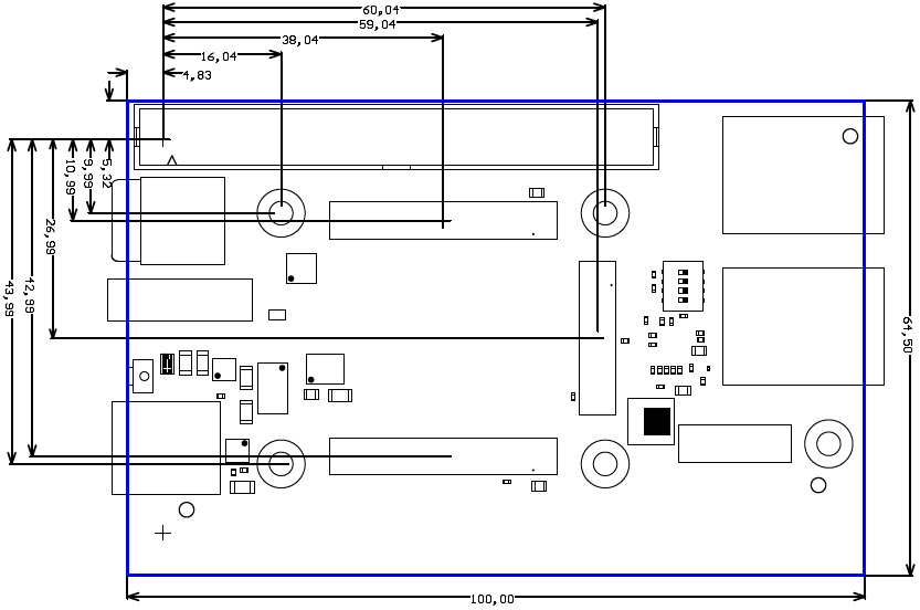
Physical Dimensions
Board size: PCB 100mm × 64.5mm. Notice that the USB type A socket on the left and the Ethernet RJ-45 jacks on the right are hanging slightly over the edge of the PCB making the total width of the longer side approximately 106mm. Please download the assembly diagram for exact numbers.
Mating height of the module with standard connectors: 8mm
PCB thickness: 1.65mm
Highest parts on the PCB are USB type A socket and the Ethernet RJ-45 jacks, approximately 15mm. Please download the step model for exact numbers.
All dimensions are given in millimeters.
Operating Temperature Ranges
Commercial grade: 0°C to +70°C.
Industrial grade: -40°C to +85°C.
Board operating temperature range depends also on customer design and cooling solution. Please contact us for options.
Weight
115g - Plain baseboard.
13g - VG96 connector.
Revision History
Hardware Revision History
| Date | Revision | Notes | PCN | Documents |
|---|---|---|---|---|
| 2016-06-28 | 02 | First production revision | - | |
- | 01 | Prototypes | - |
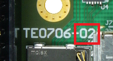
Hardware revision number is printed on the PCB board next to the module model number separated by the dash.
Document Change History
Date | Revision | Contributors | Description |
|---|---|---|---|
| 2017-01-19 | Ali Naseri, Jan Kumann | Hardware revision 02 specific changes. | |
| 2016-01-06 | V1 | Ali Naseri | Initial document. |
Disclaimer
Data Privacy
Please also note our data protection declaration at https://www.trenz-electronic.de/en/Data-protection-Privacy
Document Warranty
The material contained in this document is provided “as is” and is subject to being changed at any time without notice. Trenz Electronic does not warrant the accuracy and completeness of the materials in this document. Further, to the maximum extent permitted by applicable law, Trenz Electronic disclaims all warranties, either express or implied, with regard to this document and any information contained herein, including but not limited to the implied warranties of merchantability, fitness for a particular purpose or non infringement of intellectual property. Trenz Electronic shall not be liable for errors or for incidental or consequential damages in connection with the furnishing, use, or performance of this document or of any information contained herein.
Limitation of Liability
In no event will Trenz Electronic, its suppliers, or other third parties mentioned in this document be liable for any damages whatsoever (including, without limitation, those resulting from lost profits, lost data or business interruption) arising out of the use, inability to use, or the results of use of this document, any documents linked to this document, or the materials or information contained at any or all such documents. If your use of the materials or information from this document results in the need for servicing, repair or correction of equipment or data, you assume all costs thereof.
Copyright Notice
No part of this manual may be reproduced in any form or by any means (including electronic storage and retrieval or translation into a foreign language) without prior agreement and written consent from Trenz Electronic.
Technology Licenses
The hardware / firmware / software described in this document are furnished under a license and may be used /modified / copied only in accordance with the terms of such license.
Environmental Protection
To confront directly with the responsibility toward the environment, the global community and eventually also oneself. Such a resolution should be integral part not only of everybody's life. Also enterprises shall be conscious of their social responsibility and contribute to the preservation of our common living space. That is why Trenz Electronic invests in the protection of our Environment.
REACH, RoHS and WEEE
REACH
Trenz Electronic is a manufacturer and a distributor of electronic products. It is therefore a so called downstream user in the sense of REACH. The products we supply to you are solely non-chemical products (goods). Moreover and under normal and reasonably foreseeable circumstances of application, the goods supplied to you shall not release any substance. For that, Trenz Electronic is obliged to neither register nor to provide safety data sheet. According to present knowledge and to best of our knowledge, no SVHC (Substances of Very High Concern) on the Candidate List are contained in our products. Furthermore, we will immediately and unsolicited inform our customers in compliance with REACH - Article 33 if any substance present in our goods (above a concentration of 0,1 % weight by weight) will be classified as SVHC by the European Chemicals Agency (ECHA).
RoHS
Trenz Electronic GmbH herewith declares that all its products are developed, manufactured and distributed RoHS compliant.
WEEE
Information for users within the European Union in accordance with Directive 2002/96/EC of the European Parliament and of the Council of 27 January 2003 on waste electrical and electronic equipment (WEEE).
Users of electrical and electronic equipment in private households are required not to dispose of waste electrical and electronic equipment as unsorted municipal waste and to collect such waste electrical and electronic equipment separately. By the 13 August 2005, Member States shall have ensured that systems are set up allowing final holders and distributors to return waste electrical and electronic equipment at least free of charge. Member States shall ensure the availability and accessibility of the necessary collection facilities. Separate collection is the precondition to ensure specific treatment and recycling of waste electrical and electronic equipment and is necessary to achieve the chosen level of protection of human health and the environment in the European Union. Consumers have to actively contribute to the success of such collection and the return of waste electrical and electronic equipment. Presence of hazardous substances in electrical and electronic equipment results in potential effects on the environment and human health. The symbol consisting of the crossed-out wheeled bin indicates separate collection for waste electrical and electronic equipment.
Trenz Electronic is registered under WEEE-Reg.-Nr. DE97922676.
Overview
Content Tools