Table of Contents
Overview
The Trenz Electronic TE0701 Carrier Board is a baseboard for 4 x 5 SoMs, which exposes the module's B2B connector pins to accessible connectors and provides a whole range of on-board components to test and evaluate TE 4 x 5 SoMs.
See page "4 x 5 cm carriers" to get information about the SoMs supported by the TE0701 carrier board.
Block Diagram
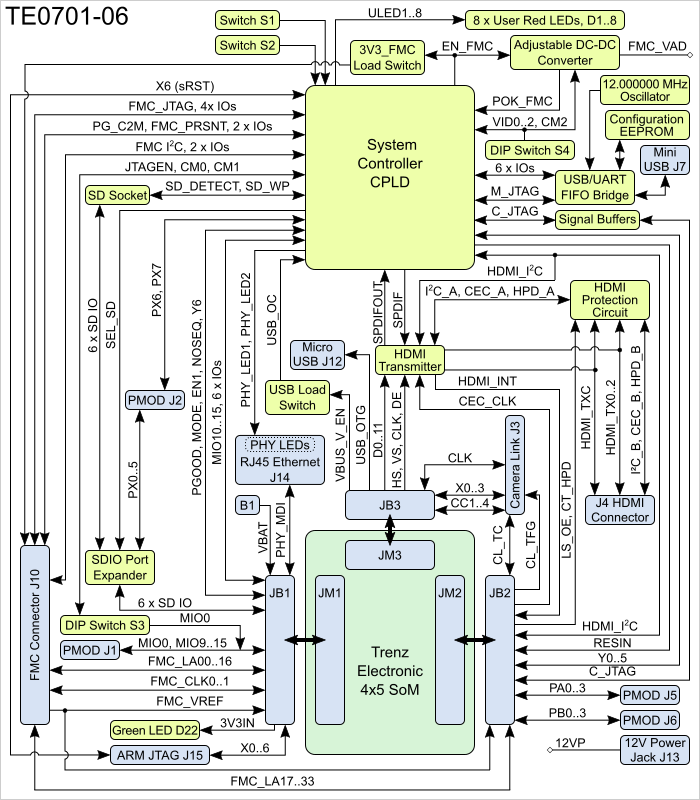
Figure 1: TE0701-06 block diagram.
Main Components
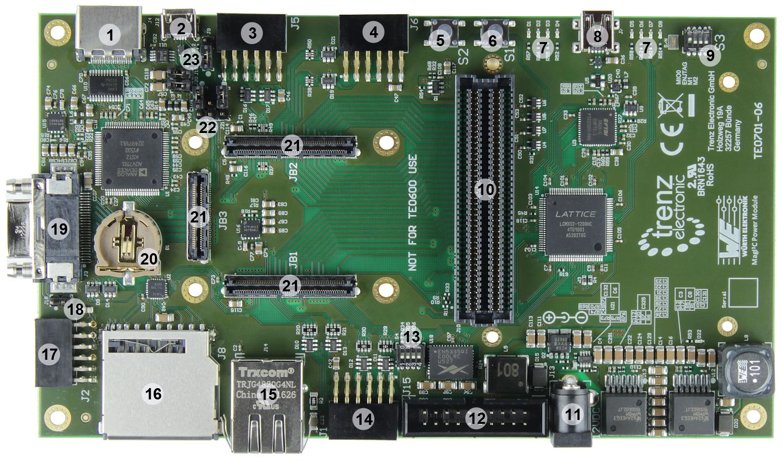
Figure 2: 4 x 5 SoM carrier board TE0701-06.
- HDMI connector (1.4 HEAC support)
- Micro-USB connector (device, host or OTG modes)
Pmod connector for access to Zynq module's PL IO-bank pins (4 LVDS pairs, max. VCCIO voltage: VIOTA)
- Pmod connector for access to Zynq module's PL IO-bank pins (4 LVDS pairs, max. VCCIO voltage: FMC_VADJ)
- User push-button S2 ("RESTART" button by default)
- User push-button S1 ("RESET" button by default)
- User LEDs (function mapping depends on firmware of System Controller CPLD)
- Mini-USB connector (USB JTAG and UART interface)
- User 4-bit DIP switch
- VITA 57.1 compliant FMC LPC connector with digitally programmable FMC VADJ power supply
- Barrel jack for 12V power supply
- ARM JTAG connector (DS-5 D-Stream) - PJTAG to EMIO multiplexing needed
- User 4-bit DIP switch (to adjust voltage of FMC_VADJ)
- Pmod connector (J1, max. VCCIO voltage: 3.3V): mapped to 8 Zynq PS MIO0 bank pins (MIO0, MIO9 to MIO15), 6 pins (MIO10 to MIO15) are additionally connected to TE0701 System Controller CPLD
- RJ45 Gigabit Ethernet connector
- SD Card connector, Zynq SDIO0 controller, can be used to boot system
- Pmod connector (J2, max. VCCIO voltage: 3.3V): 6 pins (PX0 to PX5) can be multiplexed by Texas Instruments TXS02612RTWR SDIO Port Expander to MIO pins of Zynq module, 2 pins are connected to TE0701 System Controller CPLD (PX6 and PX7)
- Jumper J18
- Mini Camera Link connector
- Battery holder for CR1220 (RTC backup voltage)
- Trenz Electronic 4 x 5 modules high-speed connector strips (3x Samtec LSHM series connectors)
- Jumper J16, J17, J21
- Jumper J9, J19, J20
Key Features
- Overvoltage-, undervoltage- and reversed- supply-voltage-protection
- Barrel jack for 12V power supply
- Carrier board System Controller CPLD Lattice MachXO2 1200HC, programmable via Mini-USB JTAG Interface J7
- Zynq module programmable via ARM JTAG interface connector (J15) or by System Controller CPLD via Mini-USB JTAG interface J7 or JTAG interface on FMC connector J10
- Mini Camera Link
- RJ45 Gigabit Ethernet MagJack with 2 integrated LEDs.
- FPGA Mezzanine Card (FMC) Connector J10 for access to Zynq module's LVDS pairs, operable with adjustable IO voltage FMC_VADJ
- USB JTAG and UART interface (FTDI FT2232HQ) with Mini-USB connector J7
- ADV7511 HDMI transmitter with HDMI connector J4
- 8 x red user LEDs routed to System Controller CPLD
- 2 x user push-button routed to System Controller CPLD. By default configured as system "RESET" and "RESTART" button (depends on CPLD firmware)
- 2 x 4-bit DIP switch for baseboard configuration (3 switches routed to System Controller CPLD, 3 switches to set voltage of FMC_VADJ, 1 switch routed to Zynq module (MIO0), 1 switch enables Mini-USB JTAG interface J7)
- Pmod connectors to access Zynq Module's LVDS pairs and MIO pins
- Micro SD card socket, can be used to boot system
- Micro-USB interface (J12) connected to Zynq module (device, host or OTG modes)
- Trenz Electronic 4 x 5 modules high-speed connector strips (3x Samtec LSHM series connectors)
Interfaces and Pins
Micro SD Card Socket
Micro SD Card socket is not directly wired to the B2B connector pins, but through a Texas Instruments TXS02612 SDIO Port Expander, which is needed for voltage translation due to different voltage levels of the Micro SD Card and MIO-bank of the Xilinx Zynq module. The Micro SD Card has 3.3V signal voltage level, but the MIO-bank on the Xilinx Zynq module has VCCIO of 1.8V.
With SD_SEL signal connected to the Texas Instruments TXS02612 SDIO Port Expander user can choose which port is accessible. Port B0 is connected to the Micro SD Card connector and B1 is connected to the Pmod J2 connector. SD_SEL signal can be controlled by the System Controller CPLD firmware.
Dual channel USB to UART/FIFO
The TE0701 carrier board has on-board high-speed USB 2.0 to UART/FIFO IC FT2232HQ from FTDI. Channel A can be used as JTAG interface (MPSSE) to program the System Controller CPLD. Channel B can be used as UART interface routed to CPLD. Also 6 additional bus-lanes are connected to the System Controller CPLD and available for user-specific use.
There is also a 256-byte serial EEPROM connected to the FT2232H chip pre-programmed with license code to support Xilinx programming tools.
Do not access the FT2232H EEPROM using FTDI programming tools, doing so will erase normally invisible user EEPROM content and invalidate stored Xilinx JTAG license. Without this license the on-board JTAG will not be accessible any more with any Xilinx tools. Software tools from FTDI website do not warn or ask for confirmation before erasing user EEPROM content.
USB Interface
The TE0701 carrier board has two physical USB connectors:
- Mini-USB connector J7 wired to on-board FTDI FT2232HQ chip.
- Micro-USB connector J12 wired to B2B connector JB3 (most of the TE 4 x 5 cm SoMs have USB transceiver on-board).
JTAG Interface
JTAG access to the System Controller CPLD and Xilinx Zynq module is provided via mini-USB JTAG interface J7 (FTDI FT2232H) and controlled by DIP switch S3-3.
The JTAG port of the System Controller CPLD is enabled by setting switch S3-3 ENJTAG to the OFF position.
LEDs
There are eight LEDs (ULED1 to ULED8) available to the user. All LEDs are red colored and connected to the on-board System Controller CPLD. Their function ls programmable and depend on the firmware of the System Controller CPLD. For detailed information, please refer to the documentation of the TE0701 System Controller CPLD.
LED5 (D5) to LED8 (D8) are operating only when the corresponding power supply VIOTB (i.e., bank 1 of the on-board System Controller CPLD) is switched on. This can be accomplished by connecting the FMC power supply FMC_VADJ to VIOTB (J21: 1,2-3), which is the default option, or by connecting either 2.5V (J17: 1,2-3) or 3.3V (J17: 1-2,3) to VIOTB (J21: 1-2,3). Please note that for the first default option, the FMC power supply voltage must be set by the user. For detailed information how to set the voltage FMC_VADJ via I2C, please refer to the documentation of the TE0701 System Controller CPLD.
Green LED D22 indicates presence of 3.3V power from the SoM attached.
4-bit DIP-switch S3
There is a 4-bit DIP-switch S3 with following default settings:
| Switch | Functionality |
|---|---|
| S3-1 | CM1: Mode pin 1 (routed to System Controller CPLD). |
| S3-2 | CM0: Mode pin 0 (routed to System Controller CPLD). |
| S3-3 | JTAGEN: Set to ON for normal JTAG operation. Has to be set to OFF position for System Controller CPLD JTAG access. |
| S3-4 | MIO0: Readable input signal by System Controller CPLD and mounted TE07xx module. |
Table 1: DIP-switch S3 settings.
User Push-buttons
On the TE0701 Carrier Board there are two push-buttons (S1 and S2) and are routed to the System Controller CPLD and available to the user. The default mapping of the push-buttons is as follows:
| Name | Default Mapping: |
|---|---|
| S1 | If S1 is pushed, the active-low RESet IN (RESIN) signal will be asserted. Note: This reset can also be forced by the FTDI USB to JTAG interface. |
| S2 | If S2 is pushed, the active-high Power ON (PON) signal (that is internally pulled-up) will be de-asserted, which can be considered as a "RESTART" function as all on-module power supplies will be switched off (except 3.3VIN) on button push and back on again on button release. The active-high PON signal is directly mapped to the active-high EN1 signal which is routed to the module's System Controller CPLD (e.g., on the TE0720) and directly used as a mandatory active-high enable signal to the power FET switch, enabling on-module 3.3V power supply output as well as all other DC-DC converters on the module. |
Table 2: Description of default functions of user push-buttons S1 and S2.
The function of the push-buttons depend on the System Controller CPLD firmware. For detailed information of the function of the push-buttons, please refer to the documentation of the TE0701 System Controller CPLD.
Ethernet
The TE0701 Carrier Board has a RJ45 Gigabit Ethernet MagJack (J14) with two LEDs. On-board Ethernet MagJack J14 pins are routed to B2B connector JB1 via MDI. The center tap of the magnetics is not connected to module's B2B connector. PHY LEDs are not connected directly to the module's B2B connectors as the 4 x 5 module have no dedicated PHY LED pins assigned. PHY LEDs are connected to the TE0701 System Controller CPLD and can be routed to some of the module's I/O pins with firmware.
See documentation of the TE0701 System Controller CPLD to get information of the function of the PHY LEDs.
Pmod Slots
J5 and J6 Pmod signal routing is done as differential pairs for pins 1-2, 3-4, 7-8 and 9-10.
Please use Master Pin-out Table table as primary reference for the pin mapping information.
Power
Power Supply
Power supply with minimum current capability of 3A at 12V for system startup is recommended.
Power-On Sequence
The on-board voltages 3.3V and 5.0V of the carrier board will be brought up simultaneously when 12V power supply is connected to the barrel jack J10.
The on-board voltages 1.8V and 2.5V will be brought up when module's 3.3V voltage level has become stable and 3.3VOUT is available on the B2B connector JB2 pins 9 and 11.
The PL IO-bank supply voltage FMC_VADJ will be available after the output of the 5.0V DC-DC converter is active and the pin EN_FMC of the System Controller CPLD is asserted.
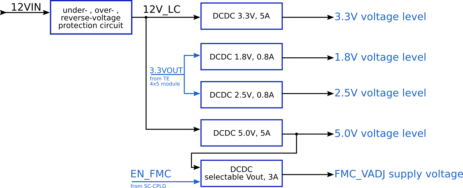
Figure 3: TE0701-06 power-up sequence diagram.
TE0701 jumper and DIP switch overview
On the TE0701 carrier board different VCCIO configurations can be chosen by 7 jumpers and one dedicated 4-bit DIP-switch S4. Settings of the jumpers and the DIP-switch S4 are explained below.
Configuring VCCIO voltage for PL IO-bank of mounted 4 x 5 SoM
The baseboard supply voltages for the PL IO-banks of the SoM are selectable by the jumpers J16, J17 and J21. The DIP-switch S4 sets the adjustable baseboard supply-voltage FMC_VADJ.
The supply-voltage FMC_VADJ is user programmable via I2C. Configuration of the adjustable voltage FMC_VADJ is done over dedicated I2C bus (lines HDMI_SCL and HDMI_SDA). A control byte has to be sent to the 8-bit control register of the I2C-to-GPIO module of the System Controller CPLD. This modules I2C address is 0x22. To enable FMC_VADJ on TE0701, bit 7 of the control register should be set to 1. Note that the I2C bus is shared with the I2C interface of the HDMI Controller.
For detailed information how to set the voltage FMC_VADJ via I2C, please refer to the documentation of the TE0701 System Controller CPLD.
There is also option to select fixed voltage of FMC_VADJ with DIP-switch S4. In this case there is no need to configure the 8-bit control register of the I2C-to-GPIO-module of the System Controller CPLD.
Switch S4 is also routed to the System Controller CPLD, hence the VCCIO configuration can be registered by the CPLD. Switch S4-4 is not dedicated for FMC_VADJ setting, the function of this switch depends on the System Controller CPLD firmware.
Table 3 below describes switch S4 settings for different FMC_VADJ voltages.
| S4-1 | S4-2 | S4-3 | FMC_VADJ Value |
|---|---|---|---|
| ON | ON | ON | 3.3V |
| OFF | ON | ON | 2.5V |
| ON | OFF | ON | 1.8V |
| OFF | OFF | ON | 1.5V |
| ON | ON | OFF | 1.25V |
Table 3: Switch S4 positions for fixed values of the FMC_VADJ voltage.
Configuring 12V Power Supply Pin on the Camera Link Connector
12V power supply can be connected to pin 26 of the CameraLink by closing J18. However, this option is disabled by default (J18: OPEN).
Configuring Power Supply of the Micro-USB Connector (device, host or OTG modes)
The TE0701 carrier board can be configured as a USB host. Hence, it must provide from 5.25V to 4.75V to the board side of the downstream connection (micro-USB port on J12; 13). To provide sufficient power, a TPS2051 power distribution switch is located on the carrier board in between the 5V power supply and the VBUS signal of the USB downstream port interface. If the output load exceeds the current-limit threshold, the TPS2051 limits the output current and pulls the over-current logic output (OC_n) low, which is routed to the on-board CPLD. The TPS2051 is put into operation by setting J19 CLOSED. J20 provides an extra 100µF decoupling capacitor (in addition to 10µF) to further stabilize the output signal. Moreover, a series terminating resistor of either 1K (J9: 1-2, 3) or 10K (J9: 1, 2-3) is selectable on the "USB-VBUS" signal. Both signals, USB-VBUS and VBUS_V_EN (that enables the TPS2051 on "high") are routed (as well as the corresponding D+/- data lines) via the on-board connector directly to the USB 2.0 high-speed transceiver PHY on the mounted SoM, which is, in turn, connected to the Zynq FPGA. In summary, the default jumper settings are the following: J9: 1-2, 3 (1K series terminating resistor); J19: CLOSED (TPS2051 in operation); J20: CLOSED (100 µF added).
Additionally, the TE0701 carrier board is equipped with a second mini-USB port (J7) which is connected to a USB to multi-purpose UART/FIFO IC from FTDI (FT2232HQ) and provides a USB to JTAG interface between a host PC and the TE0701 carrier board and the Zynq module. Because it acts as a USB function device, no power switch is required (and only a ESD protection must be provided) in this case.
Summary of VCCIO configuration via jumpers
There are two baseboard supply voltages VIOTA and VIOTB connected to the 4 x 5 SoM's PL IO-bank. The supply-voltages have following pin assignments on B2B-connectors:
Baseboard supply voltages | Baseboard B2B connector-pins | Standard assignment of PL IO-bank supply voltages on TE 4 x 5 module's B2B connectors | Baseboard voltages and signals connected with |
|---|---|---|---|
| VIOTA | JB2-2, JB2-4, JB2-6 | VCCIOB (JM2-1, JM2-3) / VCCIOC (JM2-5) | HDMI_SCL, HDMI_SDA, HDMI_INT, J5 VCCIO |
| VIOTB | JB1-10, JB1-12, JB2-8, JB2-10 | VCCIOA (JM1-9, JM1-11) / VCCIOD (JM2-7, JM2-9) | VCCIO1 (System Controller CPLD pin 55, 73) |
Table 4: Baseboard supply-voltages VIOTA and VIOTB
Note: The corresponding PL IO-voltage supply voltages of the 4 x 5 SoM to the selectable baseboard voltages VIOTA and VIOTB are depending on the mounted 4 x 5 SoM and varying in order of the used model.
Refer to SoM's schematics for more information about the specific pin assignment on module's B2B-connectors regarding PL IO-bank supply voltages and to the 4 x 5 Module integration Guide for VCCIO voltage options.
Following table describes how to configure the baseboard supply voltages with jumpers.
Baseboard supply voltages vs voltage levels | VIOTA | VIOTB | USB-VBUS | 12V0_CL |
|---|---|---|---|---|
| 3V3 | J17: 1-2, 3 & J16: open | J17: 1-2, 3 & J16: open & J21: 1-2, 3 | - | - |
| 2V5 | J17: 1, 2-3 & J16: open | J17: 1, 2-3 & J16: open & J21: 1-2, 3 | - | - |
| FMC_VADJ | J17: open & J16: 1-2 | J21: 1, 2-3 | - | - |
| 5V0 intern | - | - | J9: 1-2, 3 & J19: 1-2 (J20: 1-2: additional decoupling-capacitor 100 µF) | - |
| VBUS extern | - | - | J9: 1, 2-3 & J19: open | - |
| 12V_LC | - | - | - | J18: 1-2 |
Table 5: Configuration of baseboard supply-voltages via jumpers. 'Jx: 1-2, 3' means pins 1 and 2 are closed, pin 3 is open. 'Jx: 1, 2-3' means pins 2 and 3 are closed, pin 1 is open.
Take care of the VCCO voltage ranges of the particular PL IO-banks (HR, HP) of the mounted SoM, otherwise damages may occur to the FPGA. Therefore, refer to the TRM of the mounted SoM to get the specific information of the voltage ranges.
It is recommended to set and measure the PL IO-bank supply-voltages before mounting of TE 4 x 5 module to avoid failures and damages to the functionality of the mounted SoM.
Technical Specifications
Absolute Maximum Ratings
| Parameter | Min | Max | Units | Notes |
|---|---|---|---|---|
VIN supply voltage | 11.4 | 12.6 | V | ANSI/VITA 57.1 FPGA Mezzanine Card (FMC) standard |
Storage temperature | -55 | 125 | °C | - |
Recommended Operating Conditions
| Parameter | Min | Max | Units | Notes |
|---|---|---|---|---|
| VIN supply voltage | 11.4 | 12.6 | V | - |
Physical Dimensions
Board size: PCB 170.4 mm × 98 mm. Notice that some parts the are hanging slightly over the edge of the PCB like the mini-USB jacks (ca. 1.4 mm), the Ethernet RJ-45 jack (ca 2.2 mm) and the mini CameraLink connector (ca. 7 mm), which determine the total physical dimensions of the carrier board. Please download the assembly diagram for exact numbers.
Mating height of the module with standard connectors is 8mm.
PCB thickness: ca. 1.65mm.
Highest part on the PCB is the Ethernet RJ-45 jack, which has an approximately 17 mm overall height. Please download the step model for exact numbers.
All dimensions are given in millimeters.
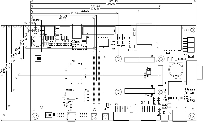
Figure 4: Physical dimensions of the TE0701-06 carrier board.
Operating Temperature Ranges
Commercial grade: 0°C to +70°C.
Board operating temperature range depends also on customer design and cooling solution. Please contact us for options.
Weight
ca. 188 g - Plain board.
Document Change History
| Date | Revision | Authors | Description |
|---|---|---|---|
| 2017-05-20 | Jan Kumann | New physical dimensions drawing of the board. | |
| 2017-05-16 | V51 | Jan Kumann | A few overall improvements and corrections, new block diagram. |
| 2017-04-11 |
| Ali Naseri | added block diagram |
| 2017-02-15 | V45 | Ali Naseri | added warning concerning the use of FTDI tools |
| 2017-02-15 | V40 | Ali Naseri | added power-on sequence diagram |
| 2017-01-19 | V35 | Ali Naseri | correction of table 3 (switch-positions to adjust FMC_VADJ) inserted hint to set and measure the PL IO-bank supply-voltages |
| 2017-01-13 | V20 | Ali Naseri | added section for baseboard supply voltage configuration |
| 2016-11-29 | V10
| Ali Naseri | TRM update due to new revision 06 of the carrier board. |
| 2016-11-28 | V4 | Ali Naseri | TRM adjustment to the newest revision (05) of TE0701 Carrier Board. |
| 2014-02-18 | 0.2 | Sven-Ole Voigt | TE0701-03 (REV3) updated |
| 2014-01-05 | 0.1 | Sven-Ole Voigt | Initial release |
| All | Sven-Ole Voigt, Ali Naseri |
Hardware Revision History
| Date | Revision | Notes | PCN | Documentation link |
|---|---|---|---|---|
| - | 06 | Additional Jumper J16 and switch S4 for setting VCCIO FMC_VADJ. | PCN-20161128 | |
| - | 05 | Improved manufacturing | TRM-TE0701-05 | |
| - | 04 | |||
| - | 03 | Changed DC/DC converters | ||
| - | 02 | Prototype | ||
| - | 01 | Prototype |
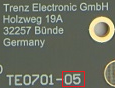
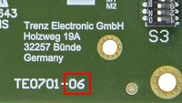
Figure 5: Hardware revision number.
Hardware revision number is printed on the PCB board next to the module model number separated by the dash.
Disclaimer
Data Privacy
Please also note our data protection declaration at https://www.trenz-electronic.de/en/Data-protection-Privacy
Document Warranty
The material contained in this document is provided “as is” and is subject to being changed at any time without notice. Trenz Electronic does not warrant the accuracy and completeness of the materials in this document. Further, to the maximum extent permitted by applicable law, Trenz Electronic disclaims all warranties, either express or implied, with regard to this document and any information contained herein, including but not limited to the implied warranties of merchantability, fitness for a particular purpose or non infringement of intellectual property. Trenz Electronic shall not be liable for errors or for incidental or consequential damages in connection with the furnishing, use, or performance of this document or of any information contained herein.
Limitation of Liability
In no event will Trenz Electronic, its suppliers, or other third parties mentioned in this document be liable for any damages whatsoever (including, without limitation, those resulting from lost profits, lost data or business interruption) arising out of the use, inability to use, or the results of use of this document, any documents linked to this document, or the materials or information contained at any or all such documents. If your use of the materials or information from this document results in the need for servicing, repair or correction of equipment or data, you assume all costs thereof.
Copyright Notice
No part of this manual may be reproduced in any form or by any means (including electronic storage and retrieval or translation into a foreign language) without prior agreement and written consent from Trenz Electronic.
Technology Licenses
The hardware / firmware / software described in this document are furnished under a license and may be used /modified / copied only in accordance with the terms of such license.
Environmental Protection
To confront directly with the responsibility toward the environment, the global community and eventually also oneself. Such a resolution should be integral part not only of everybody's life. Also enterprises shall be conscious of their social responsibility and contribute to the preservation of our common living space. That is why Trenz Electronic invests in the protection of our Environment.
REACH, RoHS and WEEE
REACH
Trenz Electronic is a manufacturer and a distributor of electronic products. It is therefore a so called downstream user in the sense of REACH. The products we supply to you are solely non-chemical products (goods). Moreover and under normal and reasonably foreseeable circumstances of application, the goods supplied to you shall not release any substance. For that, Trenz Electronic is obliged to neither register nor to provide safety data sheet. According to present knowledge and to best of our knowledge, no SVHC (Substances of Very High Concern) on the Candidate List are contained in our products. Furthermore, we will immediately and unsolicited inform our customers in compliance with REACH - Article 33 if any substance present in our goods (above a concentration of 0,1 % weight by weight) will be classified as SVHC by the European Chemicals Agency (ECHA).
RoHS
Trenz Electronic GmbH herewith declares that all its products are developed, manufactured and distributed RoHS compliant.
WEEE
Information for users within the European Union in accordance with Directive 2002/96/EC of the European Parliament and of the Council of 27 January 2003 on waste electrical and electronic equipment (WEEE).
Users of electrical and electronic equipment in private households are required not to dispose of waste electrical and electronic equipment as unsorted municipal waste and to collect such waste electrical and electronic equipment separately. By the 13 August 2005, Member States shall have ensured that systems are set up allowing final holders and distributors to return waste electrical and electronic equipment at least free of charge. Member States shall ensure the availability and accessibility of the necessary collection facilities. Separate collection is the precondition to ensure specific treatment and recycling of waste electrical and electronic equipment and is necessary to achieve the chosen level of protection of human health and the environment in the European Union. Consumers have to actively contribute to the success of such collection and the return of waste electrical and electronic equipment. Presence of hazardous substances in electrical and electronic equipment results in potential effects on the environment and human health. The symbol consisting of the crossed-out wheeled bin indicates separate collection for waste electrical and electronic equipment.
Trenz Electronic is registered under WEEE-Reg.-Nr. DE97922676.
Overview
Content Tools