Table of contents
Overview
TEC0850 design for MAX10 FPGA U18: 10M08SAU169C8G.
Feature Summary
- SC to HD-IO Bank Interface
- I²C Backplane interface
- I²C System Control interface
- Power control
- Power status
- FAN Control
- FAN Status
- Power status indication
Firmware Revision and supported PCB Revision
See Document Change History.
Product Specification
Port Description
| Name / opt. VHD Name | Direction | Pin | Bank Power | Description |
|---|---|---|---|---|
| ADBUS0 | G9 | 3V_D | ||
| ADBUS1 | F10 | 3V_D | ||
| ADBUS2 | E10 | 3V_D | ||
| ADBUS3 | D9 | 3V_D | ||
| AVDD_SHDN | G10 | 3V_D | ||
| BCBUS0 | D12 | 3V_D | ||
| BCBUS1 | E13 | 3V_D | ||
| BCBUS2 | E12 | 3V_D | ||
| BCBUS3 | F13 | 3V_D | ||
| BCBUS4 | F12 | 3V_D | ||
| BDBUS0 | B11 | 3V_D | ||
| BDBUS1 | A12 | 3V_D | ||
| BDBUS2 | B12 | 3V_D | ||
| BDBUS3 | C11 | 3V_D | ||
| BDBUS4 | B13 | 3V_D | ||
| BDBUS5 | C12 | 3V_D | ||
| BDBUS6 | C13 | 3V_D | ||
| BDBUS7 | D11 | 3V_D | ||
| CONF_DONE | C5 | 3V_D | ||
| DET_BPR | H2 | 3V_D | ||
| DET_RIO | H3 | 3V_D | ||
| DONE | N3 | PS_1V8 | ||
| EN_3V3 | C10 | 3V_D | ||
| EN_DAC1 | E6 | 3V_D | ||
| EN_DAC2 | E8 | 3V_D | ||
| EN_DAC3 | B6 | 3V_D | ||
| EN_DAC4 | A6 | 3V_D | ||
| EN_DDR | G13 | 3V_D | ||
| EN_FPD | L12 | 3V_D | ||
| EN_LPD | J13 | 3V_D | ||
| EN_PSGT | B9 | 3V_D | ||
| ERR_OUT | G5 | PS_1V8 | ||
| ERR_STATUS | H6 | PS_1V8 | ||
| F_TCK | N2 | PS_1V8 | ||
| F_TDI | M1 | PS_1V8 | ||
| F_TDO | K1 | PS_1V8 | ||
| F_TMS | J1 | PS_1V8 | ||
| F1PWM | H10 | 3V_D | ||
| F1SENSE | J9 | 3V_D | ||
| FTDI_RST | E9 | 3V_D | ||
| GA0 | F8 | 3V_D | ||
| GA0_R | F9 | 3V_D | ||
| GA1 | A2 | 3V_D | ||
| GA1_R | B2 | 3V_D | ||
| GA2 | A3 | 3V_D | ||
| GA2_R | B3 | 3V_D | ||
| GA3 | A4 | 3V_D | ||
| GA3_R | B4 | 3V_D | ||
| IEEE_SW_NC | C9 | 3V_D | ||
| IEEE_SW_NO | A11 | 3V_D | ||
| INIT_B | L2 | PS_1V8 | ||
| JTAGEN | E5 | 3V_D | ||
| LED_FP_4 | M4 | 3.3V | ||
| LP_GOOD | H13 | 3V_D | ||
| M10_RST | A7 | 3V_D | ||
| M10_RX | C2 | 3V_D | ||
| M10_TX | B1 | 3V_D | ||
| MAX_IO1 | N8 | 3.3V | ||
| MAX_IO10 | M10 | 3.3V | ||
| MAX_IO2 | N7 | 3.3V | ||
| MAX_IO3 | M9 | 3.3V | ||
| MAX_IO4 | M8 | 3.3V | ||
| MAX_IO5 | M12 | 3.3V | ||
| MAX_IO6 | M13 | 3.3V | ||
| MAX_IO7 | N9 | 3.3V | ||
| MAX_IO8 | N10 | 3.3V | ||
| MAX_IO9 | M11 | 3.3V | ||
| MIO22 | M3 | PS_1V8 | ||
| MIO23 | M2 | PS_1V8 | ||
| MIO24 | L3 | PS_1V8 | ||
| MIO25 | H5 | PS_1V8 | ||
| MR | K10 | 3V_D | ||
| N.C. | J5 | 3.3V | ||
| N.C. | J6 | 3.3V | ||
| N.C. | J7 | 3.3V | ||
| N.C. | J8 | 3.3V | ||
| N.C. | K5 | 3.3V | ||
| N.C. | K6 | 3.3V | ||
| N.C. | K7 | 3.3V | ||
| N.C. | K8 | 3.3V | ||
| N.C. | L4 | 3.3V | ||
| N.C. | L5 | 3.3V | ||
| N.C. | M5 | 3.3V | ||
| N.C. | M7 | 3.3V | ||
| N.C. | N4 | 3.3V | ||
| N.C. | N5 | 3.3V | ||
| N.C. | N6 | 3.3V | ||
| N.C. | L10 | 3.3V | ||
| N.C. | L11 | 3.3V | ||
| N.C. | N12 | 3.3V | ||
| nCONF | E7 | 3V_D | ||
| nSTATUS | C4 | 3V_D | ||
| ON_GT_L | J12 | 3V_D | ||
| ON_GT_R | K12 | 3V_D | ||
| PG_DDR | H8 | 3V_D | ||
| PG_GT_L | H9 | 3V_D | ||
| PG_GT_R | G12 | 3V_D | ||
| PG_PL | L13 | 3V_D | ||
| PG_PSGT | K11 | 3V_D | ||
| PLL_RST | K2 | PS_1V8 | ||
| PROG_B | J2 | PS_1V8 | ||
| PSON | D6 | 3V_D | ||
| RP_SCL | E1 | 3V_D | ||
| RP_SDI | G4 | 3V_D | ||
| RP_SDO | F4 | 3V_D | ||
| RP_SL | F1 | 3V_D | ||
| RST | B5 | 3V_D | ||
| RST_PRST | A8 | 3V_D | ||
| RST_PRST_R | B10 | 3V_D | ||
| RST_R | D8 | 3V_D | ||
| SATA_SCL | G2 | 3V_D | ||
| SATA_SDI | F6 | 3V_D | ||
| SATA_SDO | F5 | 3V_D | ||
| SATA_SL | G1 | 3V_D | ||
| SMB_SCL | E3 | 3V_D | ||
| SMB_SCL_R | E4 | 3V_D | ||
| SMB_SDA | C1 | 3V_D | ||
| SMB_SDA_R | D1 | 3V_D | ||
| SRST_B | H4 | PS_1V8 | ||
| SW4 | A5 | 3V_D | ||
| SYSEN | D7 | 3V_D | ||
| USR_BTN | J10 | 3V_D | ||
| WAKE | A9 | 3V_D | ||
| WAKE_R | A10 | 3V_D |
| Name / opt. VHD Name | Direction | Pin | Bank Power | Description |
|---|---|---|---|---|
| FTDI_RXD | in | UART receive data from FTDI | ||
| FTDI_TXD | out | UART transmit data to FTDI | ||
| MIO22 | out | UART receive data to FPGA | ||
| MIO23 | in | UART receive data from FPGA | ||
| ZYNQ_TDO | in | FPGA JTAG TDO | ||
| ZYNQ_TCK | out | FPGA JTAG TCK | ||
| ZYNQ_TDI | out | FPGA JTAG TDI | ||
| ZYNQ_TMS | out | FPGA JTAG TMS | ||
| ADBUS0 | in | FTDI JTAG TCK | ||
| ADBUS1 | in | FTDI JTAG TDI | ||
| ADBUS2 | out | FTDI JTAG TDO | ||
| ADBUS3 | in | FTDI JTAG TMS | ||
| USB_BTN | in | Front panel button | ||
| LED4 | out | Front panel LED4 | ||
| MR | out | Supervisor Reset output | ||
| SRST_B | out | FPGA SRST_B | ||
| FTDI_RST | out | FPGA RST_B | ||
| PLL_RST | out | Clock chip Reset | ||
| EN_DAC1 | out | DAC1 Power Enable | ||
| EN_DAC2 | out | DAC2 Power Enable | ||
| EN_DAC3 | out | DAC3 Power Enable | ||
| EN_DAC4 | out | DAC4 Power Enable | ||
| EN_FPD | out | FPD Power Enable | ||
| EN_LPD | out | LPD Power Enable | ||
| EN_DDR | out | DDR Power Enable | ||
| EN_PSGT | out | PSGT Power Enable | ||
| ON_GT_L | out | GT_L Power Enable | ||
| ON_GT_R | out | GT_R Power Enable | ||
| PG_PSGT | in | PSGT Power Good | ||
| LP_GOOD | in | LP Power Good | ||
| PG_GT_L | in | GT_L Power Good | ||
| PG_GT_R | in | GT_R Power Good | ||
| PG_PL | in | PL Power Good | ||
| PG_DDR | in | DDR Power Good | ||
| F1PWM | out | FAN PWM Control | ||
| F1SENSE | in | FAN Sense | ||
| DONE | in | FPGA DONE | ||
| IO1 | in | FPGA I2C SCL_t | ||
| IO2 | out | FPGA I2C SCL_i | ||
| IO3 | in | FPGA I2C SDA_t | ||
| IO4 | out | FPGA I2C SDA_i | ||
| IO5 | in | FPGA User LED control | ||
| SCL_R | out | SCL Strong Pull-Up Enable | ||
| SDA_R | out | SDA Strong Pull-Up Enable | ||
| SCL | inout | I2C SCL | ||
| SDA | inout | I2C SDA |
Functional Description
Power
System Controller provides control and status information for main power rails. By default all power rails are ON, the user can manipulate power using I²C interface, see Memory map table.
Reset
System controller generate a reset pulse to supervisor chip U69 when front panel button S3 is pressed.
JTAG
JTAG interface from FTDI controller passes through System Controller to FPGA.
SC to HD-IO Bank Interface
| SC I/O # | Function | FPGA IO | |
| IO1 | SCL OUT | G18 | |
| IO2 | SCL IN | G19 | |
| IO3 | SDA OUT | K18 | |
| IO4 | SDA IN | H19 | |
| IO5 | User LED | J17 | Drive SC LED, if configured in "Control Register" |
| IO6 | - | H17 | |
| IO7 | - | H18 | |
| IO8 | - | L18 | |
| IO9 | - | L17 | |
| IO10 | - | K17 |
I²C Interface
To use SC I²C interface corresponding connection should be configured in the FPGA project. There are 2 standard I²C interface controllers, which can be used AXI_IIC or Zynq UltraScale+ MPSoC integrated I²C controller.
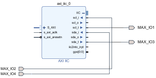
AXI_IIC
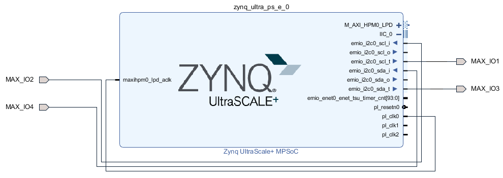
Zynq UltraScale+ MPSoC integrated I²C controller
Project XDC file should contain
set_property PACKAGE_PIN G18 [get_ports {MAX_IO1}]
set_property PACKAGE_PIN G19 [get_ports {MAX_IO2}]
set_property PACKAGE_PIN K18 [get_ports {MAX_IO3}]
set_property PACKAGE_PIN H19 [get_ports {MAX_IO4}]
set_property IOSTANDARD LVCMOS33 [get_ports MAX_IO*]
set_property PULLUP true [get_ports {MAX_IO2}]
set_property PULLUP true [get_ports {MAX_IO4}]
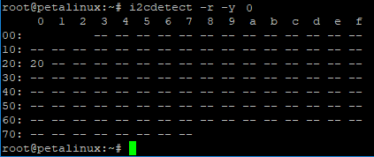
With this configuration, I²C device with address 0x20 should be visible on I²C bus
This device is an emulation of TCA6416 I²C GPIO Chip. GPIO input and output pins are used to get status and control the system.
Memory map
| Address | Register | Description |
|---|---|---|
| 0 | Input Port 0 | Power status register: Bit 0 - LP_PGOOD Bit 1 - PG_PL Bit 2 - PG_PSGT Bit 3 - PG_GT_L Bit 4 - PG_GT_R Bit 5 - PG_DDR Bit 6 - Not Used "0" Bit 7 - Not Used "0" |
| 1 | Input Port 1 | FAN Status register Bits 7:0 - FAN RPM/1000 (Nominal Sepa HFB44B-12A speed is 8000 RPM) |
| 2 | Output Port 0 | Control register 0 Bits 1:0 - LED Control (Default "01") Bit 2 - SMB Strong Pull-Up Enable (Default "1") Bit 3 - Enable DAC1 Power (Default "1") Bit 4 - Enable DAC2 Power (Default "1") Bit 5 - Enable DAC3 Power (Default "1") Bit 6 - Enable DAC4 Power (Default "1") Bit 7 - Enable FPD Power (Default "1") |
| 3 | Output Port 1 | Control register 1 Bit 0 - Enable LPD Power (Default "1") Bit 1 - Enable DDR Power (Default "1") Bit 2 - Enable PSGT Power (Default "1") Bit 3 - Enable GT_L Power (Default "1") Bit 4 - Enable GT_R Power (Default "1") Bit 5 - Enable FAN Power (Default "1") (Works only if 4-wire FAN is used) Bit 6 - Not used Bit 7 - Not used |
LED Control
| Bits [1:0] | Mode |
|---|---|
| "00" | LED4 is OFF |
| "01" | LED4 is Power indicator |
| "10" | LED4 is User LED (connected to IO5) |
| "11" | LED4 is ON |
Power Indicator
| Behavior | Description |
|---|---|
| OFF | No power or SC failure |
| 1 Pulse (*ooooooo) | PSGT Power is not OK |
| 2 Pulses (**oooooo) | DDR Power is not OK |
| 3 Pulses (***ooooo) | LP Power is not OK |
| 4 Pulses (****oooo) | GT_L Power is not OK |
| 5 Pulses (*****ooo) | GT_R Power is not OK |
| 6 Pulses (******oo) | PL Power is not OK |
| ON | No power problems detected |
I²C GPIO registers can be operated with directly, using Linux i2cset and i2cget commands
root@petalinux:~# # Disable LED4
root@petalinux:~# i2cset -y 0 0x20 2 0xFC
root@petalinux:~# # Get Power status
root@petalinux:~# i2cget -y 0 0x20 0 b
0x3f
root@petalinux:~# # Get FAN RPM/1000
root@petalinux:~# i2cget -y 0 0x20 1 b
0x08
or I²C GPIO device driver can be instantiate in Linux device tree (project-spec/meta-user/recipes-bsp/device-tree/files/system-user.dtsi).
&i2c0 {
	tca6416: tca6416@21 {
		compatible = "ti,tca6416";
		reg = <0x20>;
		gpio-controller;
		#gpio-cells = <2>;
	};
};
LED
The System Controller control D4 LED (front panel green rightmost LED). By default, it act like power status indicator see "Power Indicator" table in "I²C interface" section.
Appx. A: Change History and Legal Notices
Revision Changes
RE02 to REV03
- Add I²C GPIO core
- FAN Control/FAN Status
- Power control
Document Change History
To get content of older revision got to "Change History" of this page and select older document revision number.
| Date | Document Revision | CPLD Firmware Revision | Supported PCB Revision | Authors | Description |
|---|---|---|---|---|---|
| REV03 | REV02 |
| |||
| 2018-08-15 | v.3 | REV02 | REV02 | Antti Lukats |
|
| All |
Appx. A: Legal Notices
Overview
Content Tools