Setup of your own project
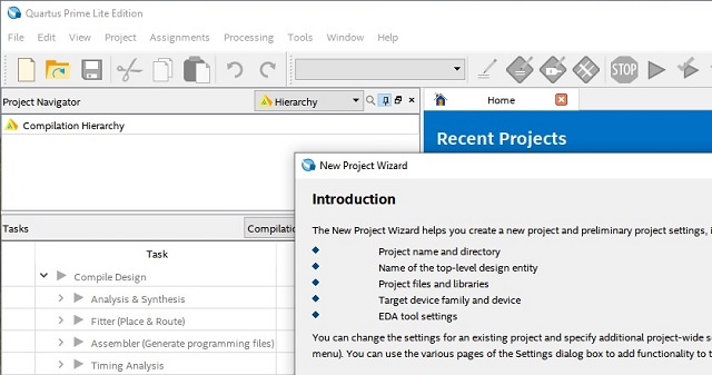
The project wizard of Quartus lite guides through the setup of a project.
Before using it, it is suggested to create a folder for the project via a file browser.
The generation of the bootloaders requires a SoC EDS Shell with root privileges on windows systems. Their file system access
is limited to the C drive. Therefore for Windows users it is best practice to store the project on the C drive.
In essence, the project setup consists of naming and placing it, and adding a device to it.
The steps in detail:
File → New Project Wizard ... setup the path to the project directory and name the project, click next.
In the following two windows Project Type and Add Files is nothing further required other than clicking next.
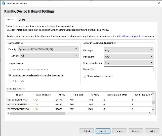
In the next window Family, Device & Board Settings it is required to select either a FPGA Device or a Board from the List.
Copy 5CSEMA5F31C8(N) into the field Name filter , this reduces the Device list, and select it in the list.
In the window EDA Tool Settings just click next and finish in the following window Summary.

Plattform Designer
File → New → Qsys System File
Program - plattform Designer opens
Upper left column - Search field type in hps
Select below: Library - Processors and Peripherals - Hard Processor Systems - Arria V/Cyclone V Hard Processor System
via double click
A new window opens
Tab FPGA Interface:
Uncheck Enable MPU standby and event signals (default)
AXI Bridges
FPGA-to-HPS interface width: unused HPS-to-FPGA interface width: unused
Lightweight HPS-to-FPGA interface width: unused
Tab Peripheral Pins:
Quad SPI Flash Controller - QSPI pin: HPS I/O Set 0
SD/MMC Controller - SDIO pin: HPS I/O Set 0 - SDIO mode: 4-bit Data
USB Controllers
SPI Controllers
UART Controllers - UART0 pin: HPS I/O Set 0 - UART0 mode: no Flow Control
I2C Controllers - I2C0 pin: HPS I/O Set 1 - I2C1 pin: HPS I/O Set 0
Can Controllers
Tab HPS Clocks:
As is / Accept the default values (for both subtabs)
Tab SDRAM - Subtask Phy Settings:
Memory clock frequency: 333.3 MHz
PLL reference clock frequency: 25 MHz
Tab SDRAM - Subtask - Memory Parameters:
Memory device speed grade: 800.0 MHz
Total interface width: 32
Row Address width: 16
Column Address width: 10
Memory Initialization Options
Memory CAS latency setting: 5
ODT Rtt nominal value: RZQ/6
Memory write CAS latency settings: 5
Tab SDRAM - Subtask - Memory Timing:
tIS (base): 180 ps tIH (base): 140 ps tDS (base) 30 ps tDH (base): 65 ps
tDQSQ: 100 ps tQH 0.38 cycles tDQSCK_ 225 ps
tDQSS: 0.27 cycles tQSH: 0.4 cycles tDSH:0.18 cycles tDSS: 0.18 cycles
tINIT: 500 us tMRD (tMRW): 4 cycles
tRAS: 35.0 ns tRCD: 13.75 ns tRP: 13.75 ns tREFI (tREFIab): 7.8 us tRFC (tRFCab): 350.0 ns tWR: 15.0 ns
tWTR: 4 cycles tFAW: 40 ns tRRD: 12.0 ns tRTP: 12.0 n
Tab SDRAM - Subtask - Board Settings:
Board Skews
Maximum CK delay to DIMM/device: 0.03
Maximum DQA delay to DIMM/device: 0.02
Minimum delay between CK and DQS: 0.09
Maximum delay between CK and DQS: 0.16
Maximum skew within DQS group: 0.01
Maximum skew between DQS groups: 0.08Average delay difference between DQ and DQA: 0.0
Maximum skew within address and command bus: 0.03Average delay difference between address and command and CK: 0.0
Bottom left → Click Finish
To change or correct these parameters later click onto the IP cores top entry in the list in the
Tab System Control - Column Name - hps_0
Add Connections via klicking into the circle MARKED with red rectangle
hps_0 - h2f_reset → clk_0 - clk_in_reset
clk_0 - clk → hps_0 - f2h_sdram0_data
Is this Step NEEDED?!?!?
Hit for good measure:
System → Assign Base Addresses
System → Assign Interrupt Numbers
System → Assign Custom Instruction Opcodes
System → Create Global Reset Network
Bottom right corner → Hit Generate HDL test
A new window opens, forcing to save the design. Give the file a name e.g. PlatformEditorHPS.qsys .
New window opens, under Synthesis, select which Hardware Language you prever Verilog ↔ VHDL
( Check - Create block symbole file (.bsf)
Click Generate and wait → Must be "Save System: completed successfully"
Hit close, Generate HDl window closes
Hit Finish, Plattform Editor window closes
FRAGE: Enable MPU Interrupts auswählen, dann muss das verbunden werden oder Exportiert, wohin / womit?
Notification opens, add file PlattformEditorHPS.qip / .sip (Not Generated, uncheckt simulate)
Add File PlattformEditorHPS.qip into Quartus via Project → Add/Remove Files in Project ...
window Settings - HPSexample opens
Hit Rectangle ... and select path:
C:\temp\Project\PlatformEditorHPS\synthesis click open
In window Settings - HPSexample click OK
In Project Navigator use the Drop-down Menu for changing from Hierarchy to Files and right click onto the
TCL script loßlassen
Tools → TCL Scripts ...
New window - TCL Scripts - opens, select
Project1 → PlatformEditorHPS → synthesis → submodules → hps_sdram_p0_pin_assignments.tcl
Click Run
When finished, new window opens, showing ... click OK
In TCL Scripts window click Close
Hit Processing → Start Compilation
Wait until the compilation has finished , this must finish without any error, warnings and critical warnings are acceptable
Overview
Content Tools