Page History
| Custom_table_size_100 |
|---|
| Page properties | ||||
|---|---|---|---|---|
| ||||
Template Revision 2.1 Design Name always "TE Series Name" + optional CPLD Name + "CPLD"
|
Overview
Firmware for PCB CPLD with designator U26 : LCMX02-256HC
Feature Summary
- Power Management
- Reset
- CPLD JTAG
- Boot Mode
- PUDC
- ETH
- LED
- I2C
Firmware Revision and supported PCB Revision
See Document Change History
Product Specification
Port Description
| Name / opt. VHD Name | Direction | Pin | Pullup/Down | Bank Power | Description |
|---|---|---|---|---|---|
| LED / LED | outOUT | 25 | NONE | 3.3VIN | Red LED D3 |
| CONFIG | outOUT | 4 | NONE | 1.8V | ETH config pin |
| EN1 / EN1 | inIN | 32 | UP | 3.3VIN | B2B Power Enable - Old name from PCB REV04 and earlier : EN1 / EN_SC3 |
| JTAGEN / --- | inIN | 26 | --- | 3.3VIN | JTAG enable for CPLD Firmware update |
| MODE /MODE | inIN | 30 | UP | 3.3VIN | B2B Boot Mode Pin- Old name from PCB REV04 and earlier : MODE /MODE_SC1 |
| MODE0_R / MODE0_R | outOUT | 12 | NONE | 3.3V | Zynq Boot Mode Pin- Old name from PCB REV04 and earlier : MODE0_R / BOOT_R0 |
| MODE2_R / MODE2_R | outOUT | 17 | NONE | 3.3V | Zynq Boot Mode Pin- Old name from PCB REV04 and earlier : MODE2_R / BOOT_R2 |
| MODE3_R / MODE3_R | outOUT | 13 | NONE | 3.3V | Zynq Boot Mode Pin- Old name from PCB REV04 and earlier : MODE3_R / BOOT_R3 |
| MR / MR | outOUT | 10 | UP | 3.3V | Zynq Reset - Old name from PCB REV04 and earlier : MR / POR_B |
| SPI_SCK_FB/VCFG1 | outOUT | 8 | NONE | 3.3V | Only for PCB REV05 and later. This pin is connected to MIO8 to change Bank 1 voltage for some applications like boundary scan to test MIOs. |
| RST / --- | --- | 9 | --- | 3.3V | / currently_not_used |
| NOSEQ / NOSEQ | inoutINOUT | 29 | UP | 3.3VIN | NOSEQ pin- Old name from PCB REV04 and earlier : NOSEQ / NOSEQ_SC4 |
| PG_3V3 / PG_3V3 | inIN | 28 | UP | 3.3VIN | Power Good- Old name from PCB REV04 and earlier : PG_3V3 / PG_1V5 |
| PG_ALL / PG_ALL | inIN | 27 | UP | 3.3VIN | Power Good - Old name from PCB REV04 and earlier: PG_DDR_PWR / PG_1V8 |
| PG_MGT / PG_MGT | inIN | 11 | NONE | 3.3V | / currently_not_usedPower Good signal of MPM3834CGPA 3.3V/1.2V_MGT power module |
| PGOOD / PGOOD | inoutINOUT | 1 | UP | 3.3VIN | B2B Power Good and additional boot mode pin(JTAG only)- Old name from PCB REV04 and earlier : PGOOD / STAT_SC2 |
| PHY_LED1 | inIN | 5 | UP | 1.8V | PHY LED Pin |
| RESIN / RESIN | inIN | 23 | UP | 3.3VIN | B2B Reset - Old name from PCB REV04 and earlier : RESIN / nRST_SC0 |
| SCL33 / SCL33 | inIN | 14 | UP | 3.3V | I2C clock pin- Old name from PCB REV04 and earlier : SCL33 / SCL |
| SDA33 / SDA33 | inoutINOUT | 16 | UP | 3.3V | I2C data pin- Old name from PCB REV04 and earlier : SDA33 / SDA |
| X0 / X0 | outOUT | 21 | NONE | VCCIO34 | FPGA Pin K8 - Old name from PCB REV04 and earlier : X0 / XA_SC |
| X1 / X1 | outOUT | 20 | NONE | VCCIO34 | PUDC FPGA Pin K7- Old name from PCB REV04 and earlier : X1 / XB_SC |
Functional Description
JTAG
JTAG signals routed directly through the CPLD to FPGA. Access between CPLD and FPGA can be multiplexed via JTAGEN pin of CPLD (pin 26) (logical one for CPLD, logical zero for FPGA). This pin is connected to B2B (JM1-pin 89) directly. On the carrier board can be this pin enabled or disabled with a dip switch.
| CPLD JTAGEN (B2B JM1-89) | Description |
|---|---|
| 0 | FPGA access |
| 1 | CPLD access |
Power
As input in CPLD PGOOD is low if if one the PG_3V3 and ,PG_ALL and ,EN1 or PG_MGT signals is low otherwise it's high impedance. PGOOD is a bidirectional signal. As output from CPLD it will be used as second boot mode selector pin. There is no additional power control.
Reset
POR_B is RESIN and (MR signal) can be extracted by anding RESIN, PG_3V3 and , PG_MGT, PG_ALL and EN1 with some delay.
PUDC
RESIN is connected to a bush button on the carrier board through B2B connector and probably a CPLD chip. It depends on which carrier bard is using.
PUDC
X1 can be changed by changing PUDC generic parameter in firmware source code. In released zip folder can be found all jed file according to PUDC state options.
Boot Mode
Boot mode can be set either by hardware (dip-switch) on the carrier board or by Linux console. Even after booting you can change the boot mode. After changing the boot mode FPGA is restarted automatically by CPLD. To change boot mode a state machine continuously monitors the corresponding register that can be change via I2C interface between CPLD and FPGA. After changing this register according to desired boot mode , CPLD will reset FPGA.
| Change Method | Boot Mode | CPLD PGOOD Pin (B2B Pin JM1-30) | CPLD MODE Pin (B2B Pin JM1-32) | Description |
|---|---|---|---|---|
| Hardware | JTAG | 0 | 0 | |
| Hardware | --- | 0 | 1 | |
| Hardware | SD Card | 1 | 0 | |
| Hardware | QSPI | 1 | 1 |
| Change Method | Boot Mode | Command in Linux console | Command in FSBL | Description |
|---|---|---|---|---|
| Software | JTAG | i2cset -y 0 0x20 0x01 0x91 | iic_write8(0x20,0x01,0x91) | 0x20 is device address. 0x1 is register address. |
| Software | SD Card | i2cset -y 0 0x20 0x01 0x93 | iic_write8(0x20,0x01,0x93) | 0x20 is device address. 0x1 is register address. |
| Software | QSPI | i2cset -y 0 0x20 0x01 0x92 | iic_write8(0x20,0x01,0x92) | 0x20 is device address. 0x1 is register address. |
ETH
CONFIG is constant zero. PHY_LED1 is connected to X0.
FSBL code
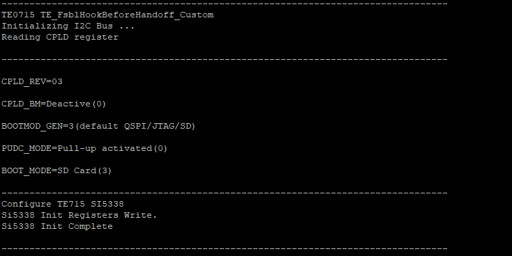
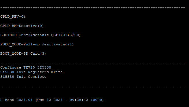
CPLD revision,Boot mode and other features of the board will be shown by FSBL code while booting.The format of these information are shown in the following:
I2C to GPIO
This subsystem provides 32-bit (4 x 8-bit) of general purpose parallel input and output (I/O) expansion for the I2C bus protocol. Address of this IP core is 0x20. This module contains four 8-bit registers for reading (GPIO_input[7:0] to GPIO_iput[31:24]) and four registers for writing (GPIO_output[7:0] to GPIO_output[31:24]) separately with 0x00 to 0x03 address. These registers can be accessed with I2C commands in linux console or with i2c functions in FSBL code. To access these registers the following commands in linux console can be used:
To see the i2c bus addresses : i2cdetect -y -r 1To read register of i2c to GPIO module: i2cget -y 1 0x20 <register address>To write data in a register of i2c to GPIO module: i2cset -y 1 0x20 <register address> <data>
| draw.io Diagram | ||||||||||||||||||||
|---|---|---|---|---|---|---|---|---|---|---|---|---|---|---|---|---|---|---|---|---|
|
I2C to GPIO is used to set boot mode in linux console or in FSBL code. It is used to activate boundary scan mode.
| Register | Direction in CPLD | Address |
|---|---|---|
| GPIO_input[7:0] | Output (reading from CPLD) | 0x00 |
| GPIO_input[15:8] | Output (reading from CPLD) | 0x01 |
| GPIO_input[23:16] | Output (reading from CPLD) | 0x02 |
| GPIO_input[31:24] | Output (reading from CPLD) | 0x03 |
| GPIO_output[7:0] | Input (writing to CPLD) | 0x00 |
| GPIO_output[15:8] | Input (writing to CPLD) | 0x01 |
| GPIO_output[23:16] | Input (writing to CPLD) | 0x02 |
| GPIO_output[31:24] | Input (writing to CPLD) | 0x03 |
NOSEQ
Noseq pin can be used by user as GPIO. In this case the following table is valid:
| NOSEQ pin as output | Condition | Command in linux console |
|---|---|---|
| '0' | GPIO_output(16) = '1' | i2cset -y 0 0x20 0x02 0x01 |
| '1' | GPIO_output(16) = '0' | i2cset -y 0 0x20 0x02 0x00 |
| NOSEQ pin as input | Description | Command in linux console |
| Reading state of NOSEQ pin | GPIO_input(16) = NOSEQ | i2cget -y 0 0x20 0x02 |
Access to CPLD registers
CPLD registers can be accessed via i2c interface. In the following table is shown how these registers can be read or written:
| Register | Direction in CPLD | Address | Related instruction in linux console |
|---|---|---|---|
| GPIO_input[7:0] | Output (reading from CPLD) | 0x00 | i2cget -y 1 0x20 0x00 |
| GPIO_input[15:8] | Output (reading from CPLD) | 0x01 | i2cget -y 1 0x20 0x01 |
| GPIO_input[23:16] | Output (reading from CPLD) | 0x02 | i2cget -y 1 0x20 0x02 |
| GPIO_input[31:24] | Output (reading from CPLD) | 0x03 | i2cget -y 1 0x20 0x03 |
| GPIO_output[7:0] | Input (writing to CPLD) | 0x00 | i2cset -y 1 0x20 0x00 <data> |
| GPIO_output[15:8] | Input (writing to CPLD) | 0x01 | i2cset -y 1 0x20 0x01 <data> |
| GPIO_output[23:16] | Input (writing to CPLD) | 0x02 | i2cset -y 1 0x20 0x02 <data> |
| GPIO_output[31:24] | Input (writing to CPLD) | 0x03 | i2cset -y 1 0x20 0x03 <data> |
The first register GPIO_input[7:0] is used to show CPLD revision.
| Register | Address | Related data | Read/Write by user | Description |
|---|---|---|---|---|
| GPIO_input[7:0] | 0x00 | CPLD REVISION (8 bits) | No | Consists of CPLD revision information |
| GPIO_input[9:8] | 0x01 | boot mode | No | Boot Mode choises for both hardware (Dip switch) and firmware (CPLD) boot mode configuration |
| GPIO_input(10) | 0x01 | Soft boot mode activation flag | No | To monitor if boot mode configuration is executed via hardware config (Dip switch) or via firmware(CPLD) |
| GPIO_input(11) | 0x01 | PUDC | No | To show PUDC state whie booting in linux console |
| GPIO_input[13:12] | 0x01 | BOOTMODE_GEN | No | The generic parameter to make various jed files. For example to generate jed file that consists of all boot mode chioses or only SD card/QSPI boot mode. |
| GPIO_input[15:14] | 0x01 | Reserved | No | "00" |
| GPIO_input(16) | 0x02 | NOSEQ pin | Yes | To read NOSEQ pin : i2cget -y 1 0x20 0x02 --> Bit 0 shows NOSEQ pin state. |
| Register | Address | related data | Description | |
| GPIO_output(16) | 0x02 | NOSEQ pin | Yes | For example to set NOSEQ pin high: i2cset -y 1 0x20 0x02 0x00 |
FSBL code
CPLD revision,boot mode and other features of the board will be shown by FSBL code in the linux console while booting.The format of these information are shown in the following:
| CPLD Revision | Software adjusted boot mode | Existed boot modes in the programmed jed File | PUDC Mode | Current boot mode | Description | |||||||
|---|---|---|---|---|---|---|---|---|---|---|---|---|
| Deactive (0) | 0 (QSPI/SD) | Pull-up activated (0) | JTAG (0) | |||||||||
| Active (1) | 1 (QSPI/JTAG) | Pull-up deactivated (1) | QSPI (2) | |||||||||
| -- | ||||||||||||
| CPLD Revision | Software adjusted boot mode | Existed boot modes in the programmed jed File | PUDC Mode | Current boot mode | Description | |||||||
| Deactive (0) | 0 (QSPI/SD) | Pull-up activated (0) | JTAG (0) | Active (1) | 1 (QSPI/JTAG) | Pull-up deactivated (1) | QSPI (2) | ---- | 2 (JTAG/SD) | ---- | SD Card (3) | |
| ---- | 3 (default QSPI/JTAG/SD) | ---- | ---- |
| Scroll Title | ||
|---|---|---|
| ||
|
Boundary scan
To implement boundary scanning (especially after the production of the board is necessary to test all MIOs), MIO bank voltage must be set to a certain value.
For more information refer to the following site :https://support.xilinx.com/s/article/57930?language=en_US
From PCB revision 05 and later MIO8 state can be changed by CPLD. According the following table the MIO bank voltage can be determined for FPGA:
| Bank Voltage | Bank 1 (related pin MIO8) | Bank 0 (related pin MIO7) | Description |
|---|---|---|---|
| 2.5V / 3.3 V | 0 | 0 | MIO8 is pulled up in module hardware. MIO7 is pulled down in module hardware. |
| 1.8 V | 1 | 1 | Default value because of pull up resistor on the board |
The bank 0 voltage is determined in 2.5V / 3.3 V for FPGA by connecting MIO7 to GND. Bank 1 voltage can be determined for FPGA by changing the state of MIO8 in linux console or in FSBL code:
| Bank 1 Voltage | Command in linux console | Command in FSBL code | Description |
|---|---|---|---|
| 2.5 V / 3.3 V | i2cset -y 0 0x20 0x01 0x61 | iic_write8(0x20,0x01,0x61) | Only for boundary scaning |
| 1.8 V | i2cset -y 0 0x20 0x01 0x64 | iic_write8(0x20,0x01,0x64) | MIO8 is set to high impedance. Because of pull up resistor on the board MIO8 will be set on high. |
As default MIO8 is set to high in the hardware to inform FPGA that bank 1 voltage is 1.8V. To implement boundary scan it is necessary to change MIO8 state to low. After changing the MIO8 state to low, FPGA will be reset and set in JTAG boot mode by CPLD automatically.
LED
| LED state | Description | Related command | ||
|---|---|---|---|---|
| Blink sequence ******** | Reset is active. (RESIN = '0') | Push reset button on the carrier board | ||
| ON | Both boot mode and MIO8 state in linux console or in FSBL code are not changed. | Default state after turning on | ||
| Blink sequence *****oooo | Boot mode is changed by software either in linux console or by FSBL code. | i2cset -y 0 0x20 0x01 0x91/i2cset -y 0 0x20 0x01 0x92/i2cset -y 0 0x20 0x01 0x93 commands in linux console | ||
| Blink sequence ***ooooo | MIO8 stateis changed in linux console or in FSBL code. | i2cset -y 0 0x20 0x01 0x61 command in linux console | ||
| Reset is active. (RESIN = '0') | Push reset button on the carrier board | |||
| Blink sequence ****oooo | Boot mode is changed by software either in linux console or by FSBL code. | ON / OFF | Controlled by user | i2cset -y 0 0x20 0x03 0xa0 → LED OFF0x01 0x91 |
Appx. A: Change History and Legal Notices
Revision Changes
0x93 commands in linux console | ||
| Blink sequence ***ooooo | MIO8 stateis changed in linux console or in FSBL code. | i2cset -y 0 0x20 0x01 0x61 command in linux console |
| ON (Default) / OFF | Both boot mode and MIO8 state in linux console or in FSBL code are not changed. LEDs can be controlled by user. | Default state after power on i2cset -y 0 0x20 0x03 0x00 → LED OFF |
Appx. A: Change History and Legal Notices
Revision Changes
- Changes REV03 to REV04
PGOOD is always 'Z', if anding of power good signals (pg) is high. In last version it is valid only , if BOOTMODE_GEN is not equal to 3.
LED status is changed from *****ooo state to ON state for default status.
LED can be controlled by user. For this purpose user should give the following commands:
LED ON (Default) --> i2cset -y 0 0x20 0x03 0x01
LED OFF --> i2cset -y 0 0x20 0x03 0x00
PG_MGT used as power good same as PG_3V3. (IN) This pin is unused in older versions.
PGOOD is always 'Z', if pg is high. In last version it is valid only , if BOOTMODE_GEN is not equal to 3.
LED status is changed from *****ooo state to ON state for default status.
LED can be controlled by user. For this purpose user should give the following commands:
LED OFF → i2cset -y 0 0x20 0x03 0xa0LED ON → i2cset -y 0 0x20 0x03 0xa1LED will not be controlled by user. → i2cset -y 0 0x20 0x03 0x00
- Changes REV02 to REV03
- Boot mode configuration via hardware (dip switch) and firmware added (Boot mode configuration via linux console)
- Pullup or pulldown states of PORT pins was checked.
- Adding i2c to gpio ip (i2c_slave.vhd)
- Changing oscillator frequency from 12.09 MHZ to 24.18MHZ
- PORT signals according to the schematic are renamed.
- JTAG time constraint correction.
- PGOOD pin is used as boot mode selector pin.
- VCFG1 (MIO8) pin can be changed by i2cset command. This pin must be grounded by boundary scanning.
Document Change History
To get content of older revision got to "Change History" of this page and select older document revision number.
| Page properties | ||||
|---|---|---|---|---|
| ||||
|
| Date | Document Revision | CPLD Firmware Revision | Supported PCB Revision | Authors | Description | ||||||||||||||||||||||
|---|---|---|---|---|---|---|---|---|---|---|---|---|---|---|---|---|---|---|---|---|---|---|---|---|---|---|---|
|
| REV04 | REV05,REV04,REV03 |
|
| ||||||||||||||||||||||
2023-06-02 | v.14 | REV03 | REV05,REV04,REV03 | John Hartfiel |
| ||||||||||||||||||||||
2022-08-08 | v.13 | REV03 | REV05,REV04,REV03 | Mohsen Chamanbaz |
| ||||||||||||||||||||||
2018-07-17 | v.6 | REV02 | REV04,REV03 | John Hartfiel |
| ||||||||||||||||||||||
| 2018-07-16 | v.1 |
| Initial release | ||||||||||||||||||||||||
| All |
|
Legal Notices
| Include Page | ||||
|---|---|---|---|---|
|
| Scroll Only | ||
|---|---|---|
|
| Scroll pdf ignore | ||||||
|---|---|---|---|---|---|---|
|
Overview
Content Tools