Page History
...
| Scroll Only (inline) |
|---|
Refer to https://wiki.trenz-electronic.de/display/PD/TE0726+TRM for online version of this manual and additional technical documentation of the product. |
The Trenz Electronic TE0726 "ZynqBerry" is a industrial-grade Raspberry Pi form-factor compatible FPGA SoM (System on Module) based on Xilinx Zynq-7010 SoC (XC7Z010 System on Chip) with up to 512 MByte DDR3L SDRAM, 4 x USB 2.0 ports, 10/100 Mbit Ethernet port and 16 MByte Flash memory.
...
| Bank | Zynq Pin | Name | Connected To |
|---|---|---|---|
| 34 | G14 | PUDC | Jumper J14 |
| 35 | G15 | DSI_XA | System Controller CPLD, pin 16 |
| 35 | F15 | DSI_XB | System Controller CPLD, pin 17 |
...
Header J8 Interface Mapping
26 PL IO and 2 MIO IOs over I2C mux. All Bank IO voltages are 3.3V.
| J8 Pin |
|---|
| Name |
|---|
| Zynq Pin | Zynq Pin | Name | J8 Pin |
|---|
| 1 |
| 3.3V |
| - |
| - |
| 5V |
| 2 |
| 3 |
| GPIO2 |
| K15 |
| - |
| 5V |
| 4 |
| 5 |
| GPIO3 |
| J14 |
| - |
| GND |
| 6 |
| 7 |
| GPIO4 |
| H12 |
| M12 |
| GPIO14 |
| 8 |
| 9 |
| GND |
| - |
| N13 |
| GPIO15 |
| 10 |
| 11 |
| GPIO17 |
| G11 |
| H11 |
| GPIO18 |
| 12 |
| 13 |
| GPIO27 |
| G12 |
| - |
| GND |
| 14 |
| 15 |
| GPIO22 |
| H13 |
| J11 |
| GPIO23 |
| 16 |
| 17 |
| 3.3V |
| - |
| K11 |
| GPIO24 |
| 18 |
| 19 |
| GPIO10 | H14 |
| - |
| GND |
| 20 |
| 21 |
| GPIO9 |
| J13 |
| K13 |
| GPIO25 |
| 22 |
| 23 |
| GPIO11 |
| J15 |
| L15 |
| GPIO8 |
| 24 |
| 25 |
| GND |
| - |
| L14 |
| GPIO7 |
| 26 |
| Page break |
|---|
Default MIO Mapping
Bank 500 MIOs
...
MIO
...
MIO0_INT
...
| 27 | MIO49(ID_SDA via TCA9544APWR) | MIO48 (ID_SCL via TCA9544APWR ) | 28 | |||
| 29 | GPIO5 | N14 | - | GND | 30 | |
| 31 | GPIO6 | R15 | M15 | GPIO12 | 32 | |
| 33 | GPIO13 | R13 | - | GND | 34 | |
| 35 | GPIO19 | R12 | L13 | GPIO16 | 36 | |
| 37 | GPIO26 | L12 | M14 | GPIO20 | 38 | |
| 39 | GND | - | P15 | GPIO21 | 40 |
Page break
Default MIO Mapping
Bank 500 MIOs
MIO | Function | Notes |
|---|---|---|
| 0 | MIO0_INT | Interrupt signal from I2C MUX. |
| 1 | SPI0_CS | SPI chip select. |
| 2 | SPI0_DQ0/M0 | Bi-directional data line 0 |
| 3 | SPI0_DQ1/M1 | Bi-directional data line 1 |
| 4 | SPI0_DQ2/M2 | Bi-directional data line 2 |
| 5 | SPI0_DQ3/M3 | Bi-directional data line 3 |
| 6 | SPI0_SCK | SPI clock. |
| 7 | MIO7 | RESETB of USB3320 chip, U18 |
| 8 | MIO8 | System Controller CPLD pin 28 |
| 9 | MIO9 | System Controller CPLD pin 29 |
| 10 | SD_D0 | Serial data 0. |
| 11 | SD_CMD | Command/Response. |
| 12 | SD_CLK | Serial clock. |
| 13 | SD_D1 | Serial data 1. |
| 14 | SD_D2 | Serial data 2. |
| 15 | SD_D3 | Serial data 3. |
Page break
Bank 501 MIOs
| MIO | Function | Notes |
|---|---|---|
| 28 | OTG-DATA4 |
| Page break |
|---|
Bank 501 MIOs
| MIO | Function | Notes | ||
|---|---|---|---|---|
| 28 | OTG-DATA4 | ULPI bi-directional data bus. | ||
| 29 | OTG-DIR | Data bus direction control signal. | ||
| 30 | OTG-STP | Data throttle signal. | ||
| 31 | OTG-NXT | Data stream stop. | ||
| 32 | OTG-DATA0 | ULPI bi-directional data bus. | ||
| 33 | OTG-DATA1 | ULPI bi-directional data bus. | ||
| 34 | OTG-DATA2 | ULPI bi-directional data bus. | ||
| 35 | OTG-DATA3 | ULPI bi-directional data bus. | ||
| 3629 | OTG-CLKDIR | Data bus direction control signalULPI clock. | ||
| 3730 | OTG-DATA5STP | Data throttle signal. | ||
| 31 | OTG-NXT | Data stream stop. | ||
| 32 | ULPI bi-directional data bus. | 38 | OTG-DATA6DATA0 | ULPI bi-directional data bus. |
| 3933 | OTG-DATA7DATA1 | ULPI bi-directional data bus. | ||
| 48 | MUX_SCL | I2C clock to I2C MUX. | ||
| 49 | MUX_SDA | I2C data to/from I2C MUX. | ||
| 52 | MIO52 | System Controller CPLD pin 20 | ||
| 53 | MIO53 | System Controller CPLD pin 21 |
On-board LEDs
There are two LEDs on TE0726 module:
...
LED
...
Color
...
Notes
...
D2
...
Red
...
4
...
CPLD bank 3.
| 34 | OTG-DATA2 | ULPI bi-directional data bus. |
| 35 | OTG-DATA3 | ULPI bi-directional data bus. |
| 36 | OTG-CLK | ULPI clock. |
| 37 | OTG-DATA5 | ULPI bi-directional data bus. |
| 38 | OTG-DATA6 | ULPI bi-directional data bus. |
| 39 | OTG-DATA7 | ULPI bi-directional data bus. |
| 48 | MUX_SCL | I2C clock to I2C MUX. |
| 49 | MUX_SDA | I2C data to/from I2C MUX. |
| 52 | MIO52 | System Controller CPLD pin 20 |
| 53 | MIO53 | System Controller CPLD pin 21 |
On-board LEDs
There are two LEDs on TE0726 module:
LED | Signal Name | Color | CPLD Pin | Notes |
|---|---|---|---|---|
| D1 | GLED | Green | 5 | CPLD bank 3. |
D2 | RLED | Red | 4 | CPLD bank 3. |
On-board Peripherals
System Controller CPLD
There is a System Controller CPLD chip LCMXO2-256HC from Lattice Semiconductor on-board. Refer to the TE0726 CPLD for more information.
Quad SPI Flash Memory
On-board QSPI flash memory (U5) on the TE0726 is provided by Cypress Semiconductor
On-board Peripherals
System Controller CPLD
There is a System Controller CPLD chip LCMXO2-256HC from Lattice Semiconductor on-board. Refer to the TE0726 CPLD for more information.
Quad SPI Flash Memory
On-board QSPI flash memory (U5) on the TE0726 is provided by Cypress Semiconductor Serial NOR Flash Memory S25FL127SABMFV10 with 128 Mbit (16 MByte) storage capacity connected to the PS MIO bank (MIO1 ... MIO6) of the Zynq SoC. This non volatile memory is used to store initial FPGA configuration. Besides FPGA configuration, remaining free flash memory can be used for user application and data storage. All four SPI data lines are connected to the FPGA Zynq PS MIO-bank allowing x1, x2 or x4 data bus widths. Maximum data rate depends on the selected bus width and clock frequency used.
Clocking
DDR3L SDRAM
The TE0726 SoM is equipped with one DDR3L-1600 SDRAM module with 1 GByte memory density. The SDRAM module is connected to the Zynq SoC's PS DDR controller with 16-bit data bus-width.
Clocking
Signal Name | Clock IC | Default | Signal Name | Clock IC | Default Frequency | Destination IC | Pin | Notes |
|---|---|---|---|---|---|---|---|---|
| PS_CLK | U14 | 33.333333 MHz | U1 | C7 | Zynq SoC system reference clock. | |||
| OSCI | U7 | 12.000000 MHz | U3 | 3 | FT2232H oscillator input. | |||
| CLK24M | U2 | 24 MHz (see also REFSEL0 .. 2) | U18 | 26 | Reference input/output clock, see datasheet. | |||
| CLK25M | U13 | 25.000000 MHz | U2 | 61 | External 25 MHz crystal input. |
...
Power and Power-On Sequence
To power-up a module, 5.0V power supply with minimum current capability of 1A is recommended.
...
Power Consumption
TE0726 needs one single power source via micro-USB jack Micro USB2.0 B socket J1. However, it is recommended to not use any USB equipment below USB standard 2.0 to power the module. Also two-pin header J5 can be used to provide power source if needed.
...
standard 2.0 to power the module. Also two-pin header J5 can be used as alternative to feed the 5V power supply voltage.
The maximum power consumption of a module mainly depends on the design which is running on the FPGA.
Xilinx provide a power estimator excel sheets to calculate power consumption. It's also possible to evaluate the power consumption of the developed design with Vivado. See also Trenz Electronic Wiki FAQ.
To power-up a module, 5.0V power supply with minimum current capability of 1A is recommended.
Power Distribution Dependencies
There is no specific power-on sequence, except to achieve minimum current draw, I/Os should be 3-stated at power-on.at power-on.
There are following dependencies how the power supply voltage (5V nominal) is distributed to the on-board DC-DC converters.
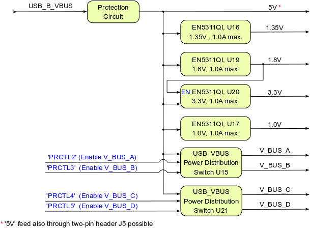
Power Rails and Bank Voltages
...
| Parameter | Min | Max | Units | Notes |
|---|---|---|---|---|
Power supply voltage J1: USB_V_BUS, J5: 5V | 4.75 | 5.5 | V | See AP2152SG-13 datasheet. |
| IOUT of AP2152SG-13 | 0 | 500 | mA | - |
| PS MIO supply voltage | 1.71 | 3.465 | V | See Xilinx DS187 datasheet |
| PS MIO input voltage | -0.2 | VCCO_MIO + 0.2 | V | VCCO_MIO0_500 and VCCO_MIO1_501. |
| PL HR I/O banks supply voltage | 1.14 | 3.465 | V | See Xilinx DS187 datasheet |
| PL HR I/O banks input voltage | -0.2 | VCCO + 0.2 | V | See Xilinx DS187 datasheet |
| Operating temperature | 0 | 70 | °C | See LAN9514 datasheet. |
The module operating temperature range depends on customer design and cooling solution. Please contact us for options.
Page break
Physical Dimensions
Module size: 40 mm × 30 mm. Please download the assembly diagram for exact numbers.
Mating height with standard connectors: 8 mm
PCB thickness: 1.6 mm
Highest part on PCB: approximately 2.5 mm. Please download the step model for exact numbers.
...
Date | Revision | Contributors | Description | ||||
|---|---|---|---|---|---|---|---|
| 2017-11-10 | John Hartfiel |
| |||||
| 2017-11-10 | v.51 | Ali Naseri |
| ||||
| 2017-05-30 | v.40 | Jan Kumann |
| 2017-05-24 | V2 | John Hartfiel | Weight. |
2017-05-24 | V1 | Jan Kumann |
|
Disclaimer
| Include Page | ||||
|---|---|---|---|---|
|
Overview
Content Tools