Page History
...
| HTML |
|---|
<!-- Download Link: Go to Base Folder of the Module or Carrier, for example : https://shop.trenz-electronic.de/en/Download/?path=Trenz_Electronic/TE0712 Use english URL "../en/.. --> |
| Scroll Ignore |
|---|
| Scroll pdf ignore | |
|---|---|
Table of Contents
|
...
Additional assembly options are available for cost or performance optimization upon request.
Block Diagram
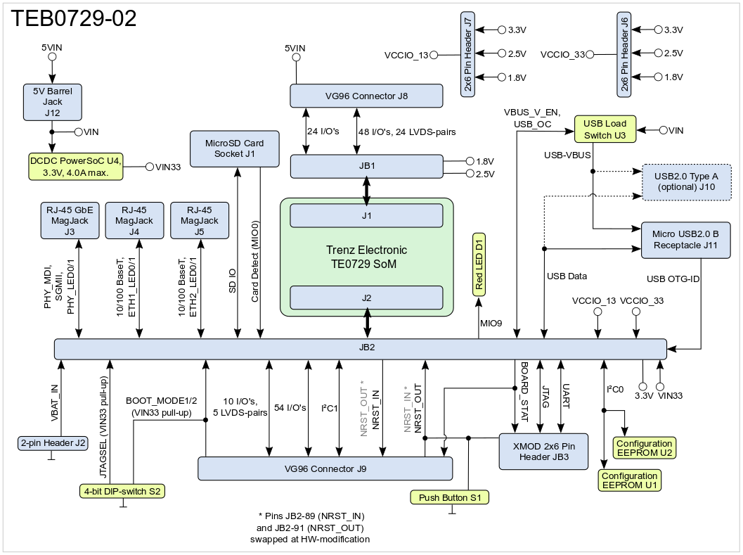
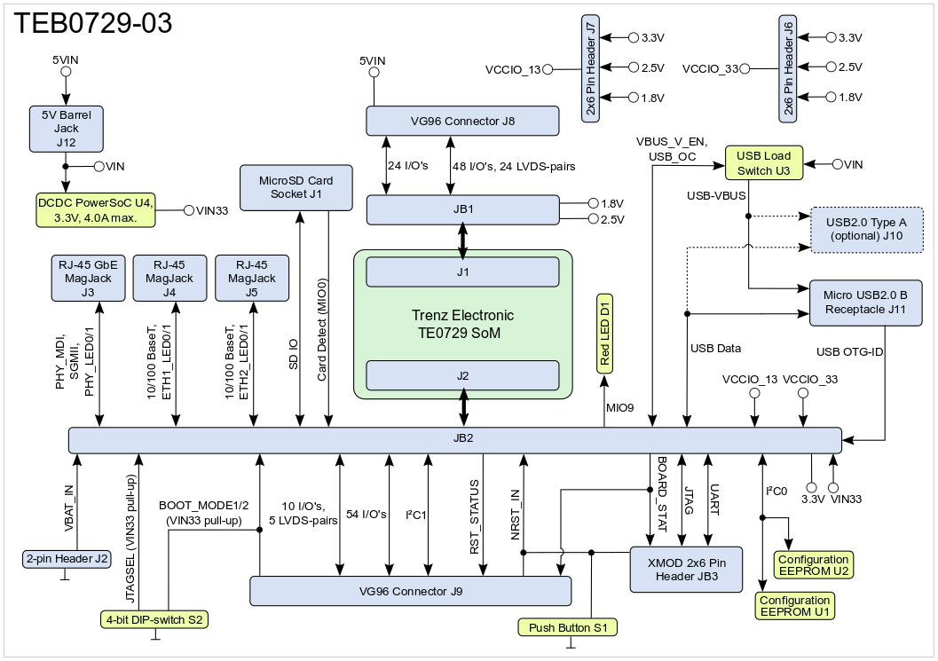
Figure 1: TEB0729-02 03 block diagram.
Main Components
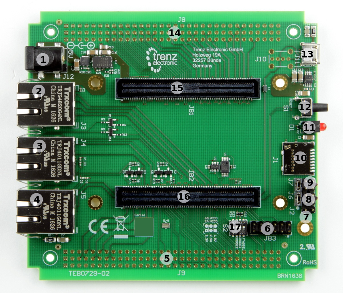
Figure 2: TEB0729-02 03 main components (picture shows PCB REV02).
- 5V barrel jack, J12
- RJ-45 Gigabit Ethernet MegJack, J3
- RJ-45 10/100-BaseT Ethernet MegJack, J4
- RJ-45 10/100-BaseT Ethernet MegJack, J5
- VG96 connector placeholder, J9
- XMOD (TE0790) header, JB3
- 2-pin header for VBAT-IN supply-voltage, J2
- 2x6 pin header for setting VCCIO_33, J6
- 2x6 pin header for setting VCCIO_13, J7
- MicroSD Card socket, J1
- Red LED, D1
- Push Button, S1
- Micro USB2.0 B Receptacle (optional USB2.0 Type A socket)
- VG96 connector placeholder, J8
- B2B Connector, JB1
- B2B Connector, JB2
- 4-bit DIP-switch, S2
...
The TEB0729 Carrier Board's Board-to-Board Connectors (B2B) have the same pin-assignment as the mounted Zynq SoM due to its hermaphroditic structure. By this connectors, the MIO- and PL-IO-bank's pins and further interfaces of the Zynq SoM can be accessed. A large quantity of these I/O's are also usable as as LVDS-pairs. The connectors provide also VCCIO voltages to operate the I/O's properly.
Following table gives a summary of the available I/O's, interfaces and LVDS-pairs of the B2B connectors JB1 and JB2:
| B2B Connector | Interfaces | Count of IO's | Interfaces | Notes |
|---|---|---|---|---|
| JB1 | User IO | 24 single ended | User IO | - |
| 48 single ended or 24 differential | User IO | - | ||
| JB2 | User IO | 54 single ended | User IO | - |
| 10 single ended or 5 differential | User IO-- | |||
| I²C | 2 | I²C | - | |
| 7 | SD IO | 7 | - | |
| UART | 2 | UART | - | 6|
| USB2.0 | 6 | - | ||
| 14 | 2x 10/100-BaseT Ethernet | 12 | - | |
| 14 | GbE MDI and SGMII | 14 | - | |
| JTAG | 4 | JTAG | - |
Table 2: General overview of PL I/O signals and SoM's interfaces connected to the B2B connectors.
...
On the VG96 connector J9 are signals assigned to control the SoM and the interfaces of the SoM's Zynq chip device and of its on-module peripherals:
Following table gives a summary of the pin-assignment, available interfaces and functional IO's of the VG96 connectors J8 and J9:
| VG96 Connector | Control Signals and Interfaces | Count of PL IO's | Count of LVDS-pairs | SoM Control Signals and Interfaces | Notes |
|---|---|---|---|---|---|
| J8 | 72 | 24 | - | - | |
| Notes | |||||
| J8 | User IO | 24 single ended | - | ||
| 48 single ended or 24 differential | - | ||||
| J9 | User IO | 54 single ended | - | ||
| 10 single ended or 5 differential | - | J9 | 64 | 5||
| 'NRST_IN' , (pin J9-A29 | Drive to ground (Push Button S1, JB3-11 (G) on XMOD header) to reset the SoM. 2) | 'NRST_OUT', ), 'RST_STATUS' (pin J9-B30Incoming reset signal from SoM's watchdog (implemented on SoM's SC CPLD). 2)) | 2 | These pins are dedicated to the specific Reset-functionality of the TE0729 SoM. | |
| 'BOARD_STAT' , (pin J9-B32) | 1 | -Frequently flipping signal indicating running SoM. Routed also to XMOD Header, pin JB3-9 (E). | |||
| 'BOOT_MODE1' , (pin J9-C31 | Bootmode pin 1, use in conjunction with Bootmode pin 2. | ), 'BOOT_MODE2' , (pin J9-C32) | Bootmode pin 2, use in conjunction with Bootmode pin 1. | 2 | Binary bootmode code of SoM, also connected to DIP S2 |
| I²C | 2I²C, pins J9-A30, J9-A31 | I²C1 interface of module. | |||
| GbE SGMII, pins J9-A16, J9-A17, J9-A19 J9-A20 | 4 | SGMII interface of on-module GbE PHY. | |||
| VG96 Connector | Count of IO's | Control Signals and Interfaces | Notes | ||
| J8 | 24 single ended | User IO | - | ||
| 48 single ended or 24 differential | User IO | - | |||
| J9 | 54 single ended | User IO | - | ||
| 10 single ended or 5 differential | User IO | - | |||
| 2 | 'NRST_IN', 'NRST_OUT', pins J9-A29, J9-B30 | SoM reset signals | |||
| 1 | 'BOARD_STAT', pin J9-B32 | - | |||
| 2 | 'BOOT_MODE1', 'BOOT_MODE2' pin J9-C31, J9-C32 | - | |||
| 2 | I²C, pins J9-A30, J9-A31 | - | |||
| 4 | GbE SGMII | - |
Table 3: General overview of PL I/O signals, SoM's interfaces and control signals connected to the VG96 connectors.
HW-modification Concerning Reset-Signals
2) The pins with the schematic net names 'NRST_IN' (JB2-89) and 'NRST_OUT' (JB2-91) are swapped as part of a HW-modification to rework the Reset-signals of the Carrier-Board in conjunction with the TE0729 SoM.
Refer to the SC CPLD documentation, section "Watchdog" to get further detailed information about the Reset-functionality of the Carrier Board and SoM before and after the HW-modification and the required SC CPLD firmware revision of the TE0729 SoM for each version of the SoM.
JTAG Interface
JTAG access to the mounted SoM is provided through B2B connector JB2 and is also routed to the XMOD header JB3. With the TE0790 XMOD USB2.0 to JTAG adapter, the Zynq chip on the mounted SoM can be programed via USB2.0 interface.
...
JTAG Signal
...
B2B Connector Pin
...
Table 4: JTAG interface signals.
UART Interface
UART interface is available on B2B connector JB2. With the TE0790 XMOD USB2.0 adapter, the UART signals can be converted to USB2.0 interface signals:
...
Table 5: UART interface signals.
I²C Interface
Two I²C interfaces are provided on B2B connector JB2. I²C0 interface is connected to the Configuration EEPROMs U1 and U2 and is dedicated to these on-board peripherals. Interface I²C1 is routed to the VG96 connector J9 and is available to the user for general purposes:
...
Table 6: I²C interface signals.
SD IO Interface
The SD IO interface of the SoM's Zynq chip (MIO-bank) is routed to the on-board MicroSD Card socket J1. By this interface, the Zynq chip can be booted from an inserted MicroSD Card:
...
Table 7: SD IO interface signals.
USB2.0 Interface
The TEB0729 Carrier Board is equipped with a Micro USB2.0 B (receptacle) socket J11 with board-revision TEB0729-02B, USB2.0 Type A socket is fitted on board-revision TEB0729-02A.
The differential data signals of the USB2.0 socket are routed to the B2B connector JB2, where they can be accessed by the USB2.0 transceiver of the mounted SoM. The USB2.0 connector can be used for Device mode, OTG Mode or Host Modes. For USB Host mode, the Carrier Board is additionally equipped with a power distribution switch U3 to provide the USB2.0 interface with the USB supply voltage USB-VBUS with nominal value of 5V. OTG mode is not available with USB2.0 Type A socket.
Following table gives an overview of the USB2.0 interface signals:
...
JB2-103
...
Table 8: USB2.0 interface signals and connections.
Gigabit Ethernet Interface
The TEB0729 Carrier Board is fitted with one RJ-45 Gigabit Ethernet Magnetic jack J3. The MegJack has two integrated LEDs (both green), its signals are routed as MDI (Media Dependent Interface) to the B2B connector JB2, where they can be accessed by the GbE PHY transceiver of the mounted SoM:
...
JB2-84
...
Table 9: GbE interface signals and connections.
...
Table 3: General overview of PL I/O signals, SoM's interfaces and control signals connected to the VG96 connectors.
JTAG Interface
JTAG access to the mounted SoM is provided through B2B connector JB2 and is also routed to the XMOD header JB3. With the TE0790 XMOD USB2.0 to JTAG adapter, the Zynq device on the mounted SoM can be programed via USB2.0 interface.
JTAG Signal | B2B Connector Pin | XMOD Header JB3 | Note |
|---|---|---|---|
| TCK | JB2-119 | JB3-4 | - |
| TDI | JB2-115 | JB3-10 | - |
| TDO | JB2-117 | JB3-8 | - |
| TMS | JB2-113 | JB3-12 | - |
| JTAGSEL | JB2-111 | - | Select SoM's JTAG programming mode on DIP-switch S2-1. |
Table 4: JTAG interface signals.
UART Interface
UART interface is available on B2B connector JB2. With the TE0790 XMOD USB2.0 adapter, the UART signals can be converted to USB2.0 interface signals:
| UART Signal Schematic Name | B2B | XMOD Header JB3 | Note |
|---|---|---|---|
| USART0_RX | JB2-94 | JB3-7 | UART receive line |
| USART0_TX | JB2-96 | JB3-3 | UART transmit line |
Table 5: UART interface signals.
I²C Interface
Two I²C interfaces are provided on B2B connector JB2. I²C0 interface is connected to the Configuration EEPROMs U1 and U2 and is dedicated to these on-board peripherals. Interface I²C1 is routed to the VG96 connector J9 and is available to the user for general purposes:
| I²C Signal Schematic Name | B2B | Connected to | Note |
|---|---|---|---|
| I2C0_SDA | JB2-90 | EEPROMs U1, U2 | I²C data line |
| I2C0_SCL | JB2-92 | EEPROMs U1, U2 | I²C clock line |
| I2C1_SDA | JB2-93 | J9-A30 | I²C data line |
| I2C1_SCL | JB2-95 | J9-A31 | I²C clock line |
Table 6: I²C interface signals.
SD IO Interface
The SD IO interface of the SoM's Zynq device (MIO-bank) is routed to the on-board MicroSD Card socket J1. By this interface, the Zynq device can be booted from an inserted MicroSD Card:
| SD IO Signal Schematic Name | B2B | Connected to | Note |
|---|---|---|---|
| ESD_DAT0 | JB2-108 | J1-7 | SD IO data |
| ESD_DAT1 | JB2-110 | J1-8 | SD IO data |
| ESD_DAT2 | JB2-100 | J1-1 | SD IO data |
| ESD_DAT3 | JB2-102 | J1-2 | SD IO data |
| ESD_CLK | JB2-106 | J1-5 | SD IO clock |
| ESD_CMD | JB2-104 | J1-3 | SD IO command |
| MIO0 | JB2-87 | J1-9 | Card Detect signal |
Table 7: SD IO interface signals.
USB2.0 Interface
The TEB0729 Carrier Board is equipped with a Micro USB2.0 B (receptacle) socket J11 with board-revision TEB0729-03B, USB2.0 Type A socket is fitted on board-revision TEB0729-03A.
The differential data signals of the USB2.0 socket are routed to the B2B connector JB2, where they can be accessed by the USB2.0 transceiver of the mounted SoM. The USB2.0 connector can be used for Device mode, OTG Mode or Host Modes. For USB Host mode, the Carrier Board is additionally equipped with a power distribution switch U3 to provide the USB2.0 interface with the USB supply voltage USB-VBUS with nominal value of 5V. OTG mode is not available with USB2.0 Type A socket.
Following table gives an overview of the USB2.0 interface signals:
| USB2.0 Signal Schematic Name | B2B | Connected to | Note |
|---|---|---|---|
| OTG-D_N | JB2-103 | J11-2, (J10-2) | USB2.0 data |
| OTG-D_P | JB2-101 | J11-3, (J10-3) | USB2.0 data |
| OTG-ID | JB2-109 | J11-4 | Ground this pin for A-Device (host), left floating this pin for B-Device (peripheral). |
| VBUS_V_EN | JB2-97 | U3, pin 4 | Enable USB-VBUS. |
| USB-VBUS | JB2-107 | J11-1, (J10-1) | USB supply voltage in Host mode. |
| USB_OC | JB2-48, J9-B29 | U3, pin 5 | USB-VBUS over current signal: current-limit threshold exceeded by the connected USB device in USB Host mode. |
Table 8: USB2.0 interface signals and connections.
Gigabit Ethernet Interface
The TEB0729 Carrier Board is fitted with one RJ-45 Gigabit Ethernet Magnetic jack J3. The MegJack has two integrated LEDs (both green), its signals are routed as MDI (Media Dependent Interface) to the B2B connector JB2, where they can be accessed by the GbE PHY transceiver of the mounted SoM:
| GbE PHY Signal Schematic Name | B2B | Connected to | Notes |
|---|---|---|---|
| PHY_MDI0_P | JB2-84 | J3-2 | - |
| PHY_MDI0_N | JB2-82 | J3-3 | - |
| PHY_MDI1_P | JB2-78 | J3-4 | - |
| PHY_MDI1_N | JB2-76 | J3-5 | - |
| PHY_MDI2_P | JB2-72 | J3-6 | - |
| PHY_MDI2_N | JB2-70 | J3-7 | - |
| PHY_MDI3_P | JB2-66 | J3-8 | - |
| PHY_MDI3_N | JB2-64 | J3-9 | - |
| PHY_LED0 | JB2-59 | Green MegJack J3 LED | - |
| PHY_LED1 | JB2-57 | Green MegJack J3 LED | - |
Table 9: GbE interface signals and connections.
For the same GbE transceiver PHY on the mounted SoM, on the Carrier Board is also SGMII (Serial Gigabit Media Independent Interface) available. The SGMII pins are available on VG96 connector J9:
| GbE PHY Signal Schematic Name | B2B | Connected to | Notes |
|---|---|---|---|
| SIN_P | JB2-52 | J9-A16 | - |
| SIN_N | JB2-54 | J9-A17 | - |
| SOUT_P | JB2-58 | J9-A19 | - |
| SOUT_N | JB2-60 | J9-A20 | - |
Table 10: GbE SGMII signals and connections.
10/100-BaseT Ethernet Interface
The TEB0729 Carrier Board is also fitted with two additional RJ-45 MegJacks providing 10/100-BaseT Ethernet interfaces. This interfaces are routed to the B2B connector JB2
| 10/100-BaseT PHY Signal Schematic Name | B2B | Connected to | Notes |
|---|---|---|---|
| ETH1_RX_P | JB2-26 | J4-3 | - |
| ETH1_RX_N | JB2-28 | J4-6 | - |
| ETH1_TX_P | JB2-20 | J4-1 | - |
| ETH1_TX_N | JB2-22 | J4-2 | - |
| ETH1_LED0 | JB2-34 | Yellow MegJack J4 LED | - |
| ETH1_LED1 | JB2-32 | Green MegJack J4 LED | - |
| ETH2_RX_P | JB2-8 | J5-3 | - |
| ETH2_RX_N | JB2-10 | J5-6 | - |
| ETH2_TX_P | JB2-2 | J5-1 | - |
| ETH2_TX_N | JB2-4 | J5-2 | - |
| ETH2_LED0 | JB2-16 | Yellow MegJack J5 LED | - |
| ETH2_LED1 | JB2-14 | Green MegJack J5 LED | - |
Table 11: 10/100-BaseT Ethernet interfaces signals and connections.
XMOD FTDI JTAG-Adapter Header
The JTAG interface of the mounted SoM can be accessed via header JB3, which has a 'XMOD FTDI JTAG Adapter'-compatible pin-assignment. So in use with the XMOD-FT2232H adapter-board TE0790 the mounted SoM can be programmed via USB interface. The TE0790 board provides also an UART interface to the Zynq SoM which can be accessed by the USB2.0 interface of the adapter-board while the signals between these serial interfaces will be converted. The adapter-board offers also two GPIO's, one with an indication LED (pin JB3-9 (E)) and another one with a low-active push button (pin JB3-11 (G)).
Following table describes the signals and interfaces of the XMOD header JB3:
| JB3 pin | Signal Schematic Net Name | B2B | Note |
|---|---|---|---|
| C (pin 4) | TCK | JB2-119 | - |
| D (pin 8) | TDO | JB2-117 | - |
| F (pin 10) | TDI | JB2-115 | - |
| H (pin 12) | TMS | JB2-113 | - |
| A (pin 3) | USART0_TX | JB2-96 | - |
| B (pin 7) | USART0_RX | JB2-94 | - |
| E (pin 9) | BOARD_STAT | JB2-112 | also connected to VG96 connector pin J9-B32 |
| G (pin 11) 2) | NRST_IN | JB2-89 | also connected to VG96 connector pin J9-A29 |
Table 12: XMOD header signals and connections. 2) Pin connected to push button S1 on XMOD FTDI JTAG Adapter
When using XMOD FTDI JTAG Adapter TE0790, the adapter-board's VCC and VCCIO will be sourced by the Carrier Board. Set the DIP-switch with the setting:
| XMOD DIP-switches | Position |
|---|---|
| Switch 1 | ON |
| Switch 2 | OFF |
| Switch 3 | OFF |
| Switch 4 | ON |
Table 13: XMOD adapter board DIP-switch positions for voltage configuration.
| Note |
|---|
Use Xilinx compatible TE0790 adapter board (designation TE0790-xx with out 'L') to program the Zynq device. The TE0790 adapter board's CPLD have to be configured with the Standard variant of the firmware. Refer to the TE0790 Resources Site for further information and firmware download. |
On-board Peripherals
| HTML |
|---|
<!--
Components on the Module, like Flash, PLL, PHY...
--> |
Configuration EEPROM
The TEB0729 Carrier Board is equipped with two Configuration EEPROMs U1 and U2 from Microchip.
- U1: Microchip 24LC128: 128 KBit memory density (8 pages a 16 KBit), 400 KHz max. clock frequency
- I²C-Address: 1010 101
- U2: Microchip 24AA025E48T: 2 KBit memory density (2 block of 128 x 8-bit words), 400 KHz max. clock frequency
- I²C-Address: 1010 011
The Configuration EEPROMs are connected to the I²C0 interface of the Zynq's MIO-bank via B2B connector JB2.
4-bit DIP-switch
Table below describes DIP-switch S2 settings for configuration of the mounted SoM:
| DIP-switches S2 | Signal Schematic Net Name | Function | Note |
|---|---|---|---|
| S2-1 | JTAGSEL | Select Zynq device or SC CPLD programming of mounted SoM: OFF: Zynq device in JTAG chain | Refer also to the TE0729 SC CPLD documentation for detailed information about JTAG update |
| S2-2 | BOOT_MODE1 | Select first bit of boot mode code | Refer to TE0729 TRM and SC CPLD documentation for detailed information about boot modes |
| S2-3 | BOOT_MODE2 | Select second bit boot mode code | |
| S2-4 | x | x | not used |
Table 14: DIP-Switch S2 SoM configuration settings
| Boot Mode | S2-2 | S2-3 |
|---|---|---|
| JTAG | ON | ON |
| SD | OFF | OFF |
| QSPI | ON | OFF |
Table 15: Boot Modes configuration via DIP-switch S2 with default TE0729 CPLD Firmware
VCCIO Selection Jumper
The Carrier Board VCCIO for the PL IO-banks of the mounted SoM are selectable by the jumpers J6 and J7.
Following table describes how to configure the VCCIO of the SoM's banks with jumpers:
| VCCIO vs. Voltage Levels | VCCIO_13 | VCCIO_33 | Note |
|---|---|---|---|
| 1.8V | J7:pins 1-2 | J6: pins 1-2 | - |
| 2.5V | J7: pins 3-4 | J6: pins 3-4 | - |
| 3.3V | J7: pins 5-6 | J6: pins 5-6 | - |
Table 16: VCCIO jumper settings.
RTC Buffer Voltage Supply Header
The buffer voltage of the SoM's RTC can be supplied through the header J2. Refer to the SoM's TRM for recommended voltage range and absolute maximum ratings.
Push Button
The Carrier Board's push button S1 is connected to the 'NRST_IN' signal, the function of the button is to trigger a reset of the mounted SoM by driving the reset-signal 'NRST_IN' to ground.
On-board LEDs
| LED | Color | Connected to | Description and Notes |
|---|---|---|---|
| D1 | Red | 'MIO9', pin JB2- 88 | user LED |
Table 17: On-board LEDs.
Power and Power-On Sequence
| HTML |
|---|
<!--
If power sequencing and distribution is not so much, you can join both sub sections together
--> |
Power Consumption
The maximum power consumption of the Carrier Board depends mainly on the mounted SoM's FPGA design running on the Zynq device.
Xilinx provide a power estimator excel sheets to calculate power consumption. It's also possible to evaluate the power consumption of the developed design with Vivado. See also Trenz Electronic Wiki FAQ.
| Power Input | Typical Current |
|---|---|
| 5VIN | TBD* |
Table 18: Typical power consumption.
* TBD - To Be Determined soon with reference design setup.
Power supply with minimum current capability of 3A for system startup is recommended.
| Warning |
|---|
| To avoid any damage to the module, check for stabilized on-board voltages and VCCIO's before put voltages on PL I/O-banks and interfaces. All I/Os should be tri-stated during power-on sequence. |
Power Distribution Dependencies
The Carrier Board needs one single power supply voltage with a nominal value of 5V. Following diagram shows the distribution of the input voltage '5VIN' to the on-board components on the mounted SoM:
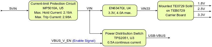
Figure 3: Board power distribution diagram.
Power Rails
The voltage direction of the power rails is directed at on-board connectors' view:
| Module Connector (B2B) Designator | VCC / VCCIO | Direction | Pins | Notes |
|---|---|---|---|---|
| JB1 | VIN33 | Out | 1, 2, 3, 4, 5, 6 | 3.3V module supply voltage |
| VCCIO_13 | Out | 101, 102 | PL IO-bank VCCIO | |
| VCCIO_33 | Out | 29, 30 | PL IO-bank VCCIO | |
| 3.3V | In | 65, 66 | voltage output from module | |
| JB2 | 1.8V | In | 49 | voltage output from module |
| 2.5V | In | 13 | voltage output from module | |
| USB-VBUS | Out | 107 | USB Host supply voltage | |
| VBAT_IN | Out | 118 | RTC buffer voltage |
Table 19: Power pin description of B2B Module Connector.
| Jumper / Header Designator | VCC / VCCIO | Direction | Pins | Notes |
|---|---|---|---|---|
| J6 | VCCIO_33 | In | 2, 4, 6 | - |
| 1.8V | Out | 5 | - | |
| 2.5V | Out | 3 | - | |
| 3.3V | Out | 1 | - | |
| J7 | VCCIO_13 | In | 2, 4, 6 | - |
| 1.8V | Out | 5 | - | |
| 2.5V | OUt | 3 | - | |
| 3.3V | Out | 1 | - |
Table 20: Power Pin description of VCCIO selection jumper pin header.
| Main Power Jack and Pins |
|---|
...
JB2-52
...
Table 10: GbE SGMII signals and connections.
10/100-BaseT Ethernet Interface
The TEB0729 Carrier Board is also fitted with two additional RJ-45 MegJacks providing 10/100-BaseT Ethernet interfaces. This interfaces are routed to the B2B connector JB2
...
JB2-26
...
Table 11: 10/100-BaseT Ethernet interfaces signals and connections.
XMOD FTDI JTAG-Adapter Header
The JTAG interface of the mounted SoM can be accessed via header JB3, which has a 'XMOD FTDI JTAG Adapter'-compatible pin-assignment. So in use with the XMOD-FT2232H adapter-board TE0790 the mounted SoM can be programmed via USB interface. The TE0790 board provides also an UART interface to the Zynq SoM which can be accessed by the USB2.0 interface of the adapter-board while the signals between these serial interfaces will be converted. The adapter-board offers also two GPIO's, one with an indication LED (pin JB3-9 (E)) and another one with a low-active push button (pin JB3-11 (G)).
Following table describes the signals and interfaces of the XMOD header JB3:
...
Table 12: XMOD header signals and connections. 3) Swapped at HW-Modification with signal 'NRST_OUT' in board-revision 2
When using XMOD FTDI JTAG Adapter TE0790, the adapter-board's VCC and VCCIO will be sourced by the Carrier Board. Set the DIP-switch with the setting:
...
Table 13: XMOD adapter board DIP-switch positions for voltage configuration.
On-board Peripherals
| HTML |
|---|
<!--
Components on the Module, like Flash, PLL, PHY...
--> |
Configuration EEPROM
The TEB0729 Carrier Board is equipped with two Configuration EEPROMs U1 and U2 from Microchip.
- U1: Microchip 24LC128: 128 KBit memory density (8 pages a 16 KBit), 400 KHz max. clock frequency
- I²C-Address: 1010 101
- U2: Microchip 24AA025E48T: 2 KBit memory density (2 block of 128 x 8-bit words), 400 KHz max. clock frequency
- I²C-Address: 1010 011
The Configuration EEPROMs are connected to the I²C0 interface of the Zynq's MIO-bank via B2B connector JB2.
4-bit DIP-switch
Table below describes DIP-switch S2 settings for configuration of the mounted SoM:
...
Select Zynq chip or SC CPLD programming of mounted SoM:
OFF: Zynq chip programming.
ON: SC CPLD programming
...
Table 14: DIP-Switch S2 SoM configuration settings.
TE0729 Bootmodes
If TE0729 is mounted, following bootmodes can be configured by setting the DIP-switches S2-2 and S2-3:
...
Table 15: Bootmode configuration via DIP-switch S2.
The selected bootmode via DIP-switch S2 depends also on the current configured SC CPLD firmware on the mounted SoM and may vary.
VCCIO Setting Jumper
The Carrier Board VCCIO for the PL IO-banks of the mounted SoM are selectable by the jumpers J6 and J7.
Following table describes how to configure the VCCIO of the SoM's banks with jumpers:
...
Table 16: VCCIO jumper settings.
RTC Buffer Voltage Supply Header
The buffer voltage of the SoM's RTC can be supplied through the header J2. Refer to the SoM's TRM for recommended voltage range and absolute maximum ratings.
Push Button
The Carrier Board's push button S1 is connected to the 'NRST_IN' signal, the function of the button is to trigger a reset of the mounted SoM by driving the reset-signal 'NRST_IN' to ground.
On-board LEDs
...
Table 17: On-board LEDs.
Power and Power-On Sequence
| HTML |
|---|
<!--
If power sequencing and distribution is not so much, you can join both sub sections together
--> |
Power Consumption
The maximum power consumption of the Carrier Board depends mainly on the mounted SoM's FPGA design running on the Zynq chip.
Xilinx provide a power estimator excel sheets to calculate power consumption. It's also possible to evaluate the power consumption of the developed design with Vivado. See also Trenz Electronic Wiki FAQ.
...
Table 18: Typical power consumption.
* TBD - To Be Determined soon with reference design setup.
Power supply with minimum current capability of 3A for system startup is recommended.
| Warning |
|---|
| To avoid any damage to the module, check for stabilized on-board voltages and VCCIO's before put voltages on PL I/O-banks and interfaces. All I/Os should be tri-stated during power-on sequence. |
Power Distribution Dependencies
The Carrier Board needs one single power supply voltage with a nominal value of 5V. Following diagram shows the distribution of the input voltage '5VIN' to the on-board components on the mounted SoM:
Figure 3: Board power distribution diagram.
Power Rails
| Module Connector (B2B) Designator | VCC / VCCIO | Direction | Pins | Notes |
|---|---|---|---|---|
| J12 | VIN335VIN | OutIn | Pin 1, 2, 3, 4, 5, 6 | 3.3V module supply voltage |
| VCCIO_13 | Out | Pin 101, 102 | PL IO-bank VCCIO | |
| VCCIO_33 | Out | Pin 29, 30 | PL IO-bank VCCIO | |
| 3.3V | In | Pin 65, 66 | voltage output from module | |
| JB2 | 1.8V | In | Pin 49 | voltage output from module |
| 2.5V | In | Pin 13 | voltage output from module | |
| USB-VBUS | Out | Pin 107 | USB Host supply voltage | |
| VBAT_IN | Out | Pin 118 | RTC buffer voltage |
Table 19: Power pin description of B2B Module Connector.
1 | - | |||
| J9 | 5VIN | In / Out | A1, A2 | also usable as '5VIN' power supply to the Carrier Board as alternative to J12 |
| J2 | VBAT_IN | In | 1 | Attention: Pin 2 connected to ground. VBAT_IN voltage on this pin cause short-circuit. |
Table 21: Main Power jack and pins description.
| Peripheral Socket Designator | VCC / VCCIO | Direction | Pins | Notes |
|---|---|---|---|---|
| J10 / J11 | USB-VBUS | In / Out | 1 | Direction depends on USB2.0 mode |
| J1 | VIN33 | Out | 4 | MikroSD Card socket VDD |
Table 22: Power pin description of peripheral connector.
| XMOD Jumper / Header Designator | VCC / VCCIO | Direction | Pins | Notes | |||
|---|---|---|---|---|---|---|---|
| J6 | VCCIO_33 | Out | Pin 2, 4, 6 | - | |||
| 1.8V | In | 5 | - | ||||
| 2.5V | In | 3 | -JB3 | 3.3V | In- | 15 | -not connected |
| VIO | VCCIO_13 | Out | Pin 2, 4, 6 | - | |||
| 1.8V | In | 5 | - | ||||
| 2.5V | In | 3 | - | ||||
| 3.3V | In | 1 | - |
Table 20: Power Pin description of VCCIO selection jumper pin header.
...
-
...
| 6 | connected to VIN33 |
Table 23: Power pin description of XMOD/JTAG Connector.
Board to Board Connectors
The TE0729 module has two 120-pin double-row REF-189019-02 connectors on the bottom side which are compatible with Samtec BSE-060-01-L-D-A connectors. Mating connectors on the baseboard are REF-189019-01, which are compatible with Samtec BTE-060-01-L-D-A connectors.
Order | REF Number | Samtec Number | Type | Mated Height | Data sheet | Comment |
|---|---|---|---|---|---|---|
| - | REF-189019-02 | BTE-060-01-L-D-A-K-TR | Module connector | 5 mm | http://suddendocs.samtec.com/catalog_english/bte.pdf | Standard connector used on module |
| 26663 | REF-189019-01 | BSE-060-01-L-D-A-TR | Baseboard connector | 5 mm | http://suddendocs.samtec.com/catalog_english/bse.pdf | Standard connector used on board |
Table 24: B2B Connectors.
| Connector Specifications | Value |
|---|---|
| Insulator material | Liquid crystal polymer |
| Stacking height | 5 mm |
| Contact material | Phosphor-bronze |
| Plating | Au or Sn over 50 μ" (1.27 μm) Ni |
| Current rating | 2 A per pin (1 pin powered per row) |
| Operating temperature range | -55 °C to +125 °C |
| Voltage rating | 225 VAC with 5 mm stack height |
| Max cycles | 100 |
| RoHS compliant | Yes |
Table 25: B2B Connector specifications.
Table 21: Main Power jack and pins description.
...
Table 22: Power pin description of peripheral connector.
...
Table 23: Power pin description of XMOD/JTAG Connector.
Board to Board Connectors
Include Page
Variants Currently In Production
| Module Variant | Operating Temperature | USB Socket | Temperature Range |
|---|---|---|---|
| TEB0729-0203-A | -40°C to +125°C | USB2.0 Type A socket fitted | Industrial |
| TEB0729-0203-B | -40°C to +125°C | Micro USB2.0 B socket fitted | Industrial |
Table 2426: Module Board variants.
Technical Specifications
...
Parameter | Min | Max | Units | Reference Document |
|---|---|---|---|---|
5VIN supply voltage | -0.3 | 7 | V | MP5010A, EN6347QI data sheet |
Storage temperature | -65 | 150 | °C | - |
Table 2527: Module absolute maximum ratings.
...
| Parameter | Min | Max | Units | Reference Document |
|---|---|---|---|---|
| 5VIN supply voltage | 4.75 | 5.25 | V | USB2.0 specification concerning 'VBUS' voltage |
| Operating temperature | -40 | 125 | °C | - |
Table 2628: Module recommended operating conditions.
...
Hardware Revision History
| Date | Revision | Notes | PCNSchematic Change Notes | Documentation Link | Note | ||||||
|---|---|---|---|---|---|---|---|---|---|---|---|
| - | 01 |
| - | TEB0729-01 | First Production Release | -||||||
| - | 02 |
| - | TEB0729-0102 | |||||||
| - | - | 02 | Second Production Release | - | 03 |
| TEB0729-02 | HW-Modification since 22.08.2017 |
| - | TEB0729-03 |
Table 29Table 27: Module hardware revision history.
...
Date | Revision | Contributors | Description | ||||||||
|---|---|---|---|---|---|---|---|---|---|---|---|
| Ali Naseri |
| |||||||||
2017-10-27 | v.14 | Ali Naseri |
|
Table 2830: Document change history.
...
Overview
Content Tools