Download PDF version of this document.
Table of Contents
Overview
The Trenz Electronic TEB0729 is a Carrier Board designed especially for the TE0729 Zynq-7000 SoM. The board exposes the module's B2B connector pins to accessible connectors and provides on-board peripheral components to test and evaluate TE Zynq-7000 SoMs and for developing purposes..
The Carrier Board provides soldering-pads for VG96 connectors as place-holders to get access to the PL-IO-banks and other functional units of the mounted SoM.
Key Features
- Barrel jack for 5V power supply
- 2x RJ45 10/100-BaseT Ethernet MagJack with 2 integrated LEDs
- 1x RJ45 Gigabit Ethernet MagJack with 2 integrated LEDs.
- 2x Configuration EEPROM's, connected to SoM's I²C interface
- XMOD compatible header to connect the TE0790 USB2.0 adapter board
- JTAG and UART interface over XMOD header
- MicroSD Card socket, can be used to boot system
- USB2.0 socket (Option: USB Type A or Micro USB2.0 B)
- 4-bit DIP switch for SoM configuration (SoM's JTAG access and Bootmode)
- VG96 connector soldering-pads J8 for access to SoM's PL-IO-bank-pins, usable as LVDS-pairs
- VG96 connector soldering-pads J9 for access to further interfaces and IO's of the SoM
- 1 x user LED (red) routed to SoM
- 1 x user push-button routed to SoM (Reset function at standard configuration)
- Pin headers to set PL-IO-bank's VCCIO with jumper
Additional assembly options are available for cost or performance optimization upon request.
Block Diagram
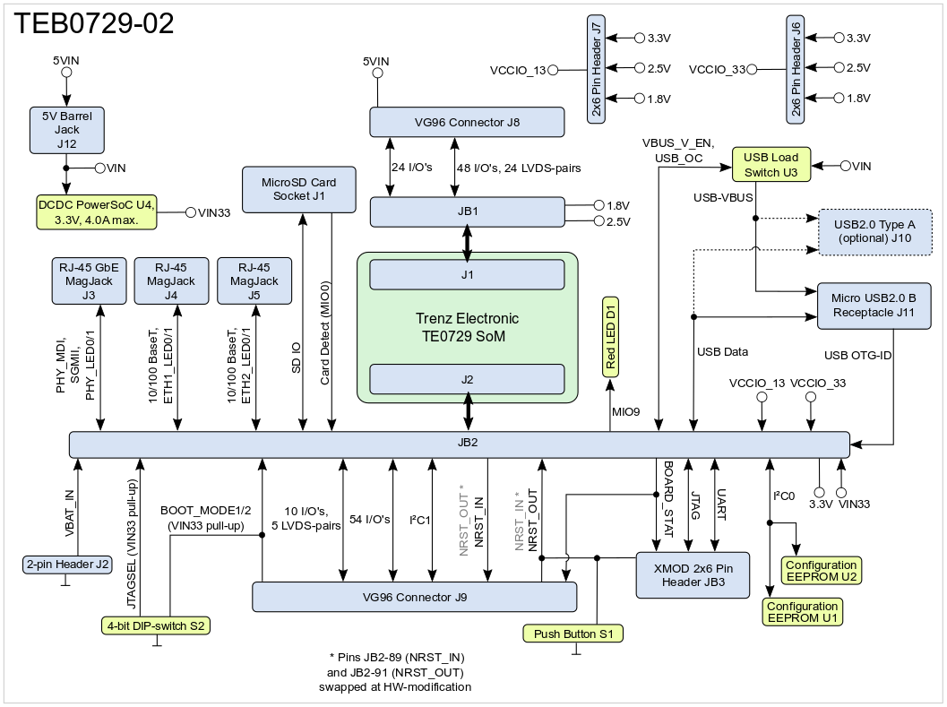
Figure 1: TEB0729-02 block diagram.
Main Components
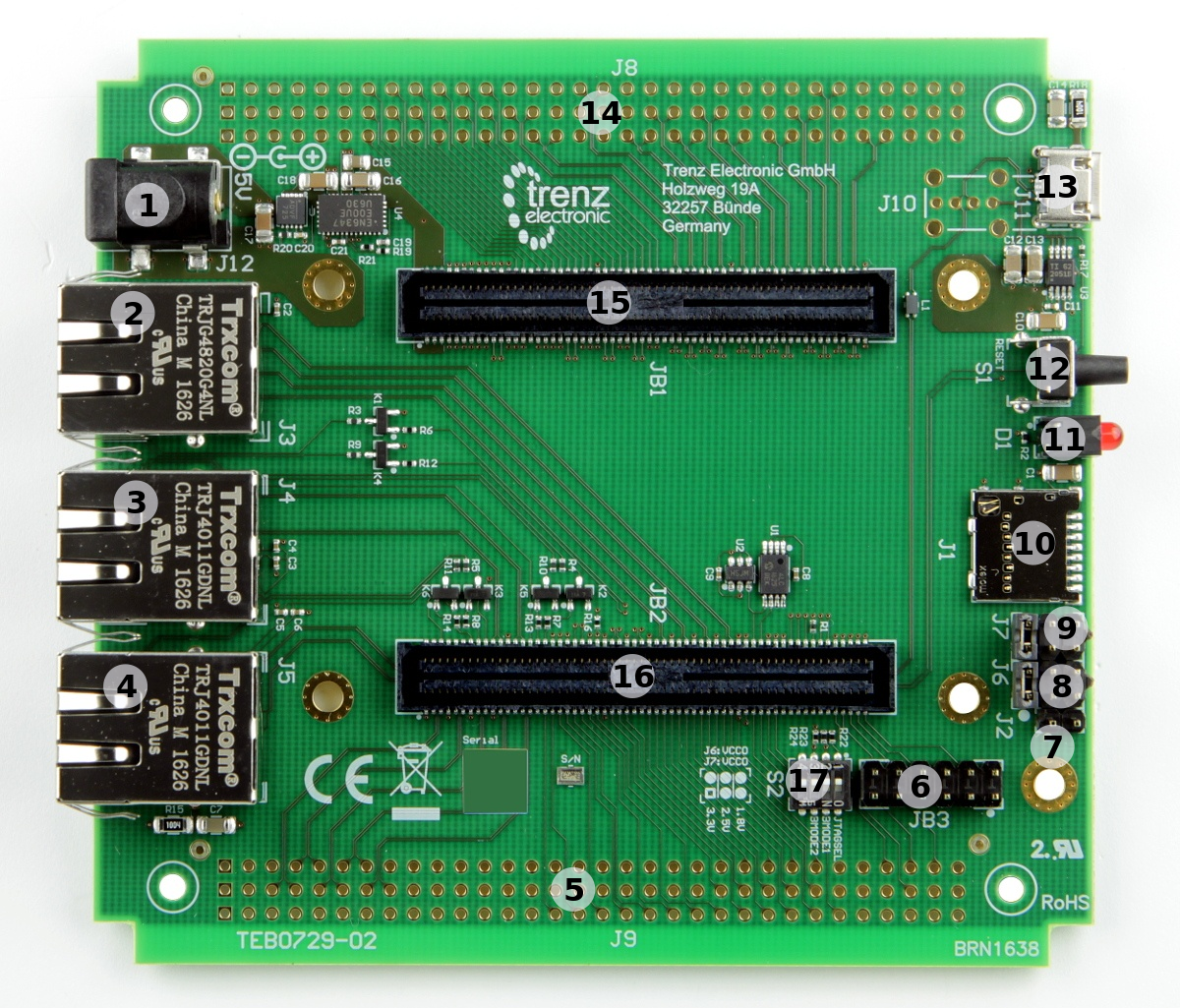
Figure 2: TEB0729-02 main components.
- 5V barrel jack, J12
- RJ-45 Gigabit Ethernet MegJack, J3
- RJ-45 10/100-BaseT Ethernet MegJack, J4
- RJ-45 10/100-BaseT Ethernet MegJack, J5
- VG96 connector placeholder, J9
- XMOD (TE0790) header, JB3
- 2-pin header for VBAT-IN supply-voltage, J2
- 2x6 pin header for setting VCCIO_33, J6
- 2x6 pin header for setting VCCIO_13, J7
- MicroSD Card socket, J1
- Red LED, D1
- Push Button, S1
- Micro USB2.0 B Receptacle (optional USB2.0 Type A socket)
- VG96 connector placeholder, J8
- B2B Connector, JB1
- B2B Connector, JB2
- 4-bit DIP-switch, S2
Initial Delivery State
Storage device name | Content | Notes |
|---|---|---|
| Configuration EEPROM, U1 | Empty | Not programmed |
| Configuration EEPROM, U2 | Empty | Not programmed |
Table 1: Initial delivery state of programmable devices on the module.
Signals, Interfaces and Pins
B2B Connector
The TEB0729 Carrier Board's Board-to-Board Connectors (B2B) have the same pin-assignment as the mounted Zynq SoM due to its hermaphroditic structure. By this connectors, the MIO- and PL-IO-bank's pins and further interfaces of the Zynq SoM can be accessed. A large quantity of these I/O's are also usable as LVDS-pairs. The connectors provide also VCCIO voltages to operate the I/O's properly.
Following table gives a summary of the available I/O's, interfaces and LVDS-pairs of the B2B connectors JB1 and JB2:
| B2B Connector | Count of IO's | Interfaces | Notes |
|---|---|---|---|
| JB1 | 24 single ended | User IO | - |
| 48 single ended or 24 differential | User IO | - | |
| JB2 | 54 single ended | User IO | - |
| 10 single ended or 5 differential | User IO | - | |
| 2 | I²C | - | |
| 7 | SD IO | - | |
| 2 | UART | - | |
| 6 | USB2.0 | - | |
| 14 | 2x 10/100-BaseT Ethernet | - | |
| 14 | GbE MDI and SGMII | - | |
| 4 | JTAG | - |
Table 2: General overview of PL I/O signals and SoM's interfaces connected to the B2B connectors.
VG96 Connector
The TEB0729 Carrier Board has soldering pads provides as place-holders to mount VG96 connectors J8 and J9 to get access the PL-IO-bank's pins and further interfaces of the Zynq SoM. With mounted VG96 connectors, SoM's IO's are available to the user, a large quantity of these I/O's are also usable as LVDS-pairs.
On the VG96 connector J9 are signals assigned to control the SoM and the interfaces of the SoM's Zynq chip and of its on-module peripherals:
Following table gives a summary of the pin-assignment, available interfaces and functional IO's of the VG96 connectors J8 and J9:
| VG96 Connector | Count of PL IO's | Count of LVDS-pairs | SoM Control Signals and Interfaces | Notes |
|---|---|---|---|---|
| J8 | 72 | 24 | - | - |
| J9 | 64 | 5 | 'NRST_IN', pin J9-A29 | Drive to ground (Push Button S1, JB3-11 (G) on XMOD header) to reset the SoM. 2) |
| 'NRST_OUT', pin J9-B30 | Incoming reset signal from SoM's watchdog (implemented on SoM's SC CPLD). 2) | |||
| 'BOARD_STAT', pin J9-B32 | Frequently flipping signal indicating running SoM. Routed also to XMOD Header, pin JB3-9 (E). | |||
| 'BOOT_MODE1', pin J9-C31 | Bootmode pin 1, use in conjunction with Bootmode pin 2. | |||
| 'BOOT_MODE2', pin J9-C32 | Bootmode pin 2, use in conjunction with Bootmode pin 1. | |||
| I²C, pins J9-A30, J9-A31 | I²C1 interface of module. | |||
| GbE SGMII, pins J9-A16, J9-A17, J9-A19 J9-A20 | SGMII interface of on-module GbE PHY. |
| VG96 Connector | Count of IO's | Control Signals and Interfaces | Notes |
|---|---|---|---|
| J8 | 24 single ended | User IO | - |
| 48 single ended or 24 differential | User IO | - | |
| J9 | 54 single ended | User IO | - |
| 10 single ended or 5 differential | User IO | - | |
| 2 | 'NRST_IN', 'NRST_OUT', pins J9-A29, J9-B30 | SoM reset signals | |
| 1 | 'BOARD_STAT', pin J9-B32 | - | |
| 2 | 'BOOT_MODE1', 'BOOT_MODE2' pin J9-C31, J9-C32 | - | |
| 2 | I²C, pins J9-A30, J9-A31 | - | |
| 4 | GbE SGMII | - |
Table 3: General overview of PL I/O signals, SoM's interfaces and control signals connected to the VG96 connectors.
HW-modification Concerning Reset-Signals
2) The pins with the schematic net names 'NRST_IN' (JB2-89) and 'NRST_OUT' (JB2-91) are swapped as part of a HW-modification to rework the Reset-signals of the Carrier-Board in conjunction with the TE0729 SoM.
Refer to the SC CPLD documentation, section "Watchdog" to get further detailed information about the Reset-functionality of the Carrier Board and SoM before and after the HW-modification and the required SC CPLD firmware revision of the TE0729 SoM for each version of the SoM.
JTAG Interface
JTAG access to the mounted SoM is provided through B2B connector JB2 and is also routed to the XMOD header JB3. With the TE0790 XMOD USB2.0 to JTAG adapter, the Zynq chip on the mounted SoM can be programed via USB2.0 interface.
JTAG Signal | B2B Connector Pin | XMOD Header JB3 | Note |
|---|---|---|---|
| TCK | JB2-119 | JB3-4 | - |
| TDI | JB2-115 | JB3-10 | - |
| TDO | JB2-117 | JB3-8 | - |
| TMS | JB2-113 | JB3-12 | - |
| JTAGSEL | JB2-111 | - | Select SoM's JTAG programming mode on DIP-switch S2-1. |
Table 4: JTAG interface signals.
UART Interface
UART interface is available on B2B connector JB2. With the TE0790 XMOD USB2.0 adapter, the UART signals can be converted to USB2.0 interface signals:
| UART Signal Schematic Name | B2B | XMOD Header JB3 | Note |
|---|---|---|---|
| USART0_RX | JB2-94 | JB3-7 | UART receive line |
| USART0_TX | JB2-96 | JB3-3 | UART transmit line |
Table 5: UART interface signals.
I²C Interface
Two I²C interfaces are provided on B2B connector JB2. I²C0 interface is connected to the Configuration EEPROMs U1 and U2 and is dedicated to these on-board peripherals. Interface I²C1 is routed to the VG96 connector J9 and is available to the user for general purposes:
| I²C Signal Schematic Name | B2B | Connected to | Note |
|---|---|---|---|
| I2C0_SDA | JB2-90 | EEPROMs U1, U2 | I²C data line |
| I2C0_SCL | JB2-92 | EEPROMs U1, U2 | I²C clock line |
| I2C1_SDA | JB2-93 | J9-A30 | I²C data line |
| I2C1_SCL | JB2-95 | J9-A31 | I²C clock line |
Table 6: I²C interface signals.
SD IO Interface
The SD IO interface of the SoM's Zynq chip (MIO-bank) is routed to the on-board MicroSD Card socket J1. By this interface, the Zynq chip can be booted from an inserted MicroSD Card:
| SD IO Signal Schematic Name | B2B | Connected to | Note |
|---|---|---|---|
| ESD_DAT0 | JB2-108 | J1-7 | SD IO data |
| ESD_DAT1 | JB2-110 | J1-8 | SD IO data |
| ESD_DAT2 | JB2-100 | J1-1 | SD IO data |
| ESD_DAT3 | JB2-102 | J1-2 | SD IO data |
| ESD_CLK | JB2-106 | J1-5 | SD IO clock |
| ESD_CMD | JB2-104 | J1-3 | SD IO command |
| MIO0 | JB2-87 | J1-9 | Card Detect signal |
Table 7: SD IO interface signals.
USB2.0 Interface
The TEB0729 Carrier Board is equipped with a Micro USB2.0 B (receptacle) socket J11 with board-revision TEB0729-02B, USB2.0 Type A socket is fitted on board-revision TEB0729-02A.
The differential data signals of the USB2.0 socket are routed to the B2B connector JB2, where they can be accessed by the USB2.0 transceiver of the mounted SoM. The USB2.0 connector can be used for Device mode, OTG Mode or Host Modes. For USB Host mode, the Carrier Board is additionally equipped with a power distribution switch U3 to provide the USB2.0 interface with the USB supply voltage USB-VBUS with nominal value of 5V. OTG mode is not available with USB2.0 Type A socket.
Following table gives an overview of the USB2.0 interface signals:
| USB2.0 Signal Schematic Name | B2B | Connected to | Note |
|---|---|---|---|
| OTG-D_N | JB2-103 | J11-2, (J10-2) | USB2.0 data |
| OTG-D_P | JB2-101 | J11-3, (J10-3) | USB2.0 data |
| OTG-ID | JB2-109 | J11-4 | Ground this pin for A-Device (host), left floating this pin for B-Device (peripheral). |
| VBUS_V_EN | JB2-97 | U3, pin 4 | Enable USB-VBUS. |
| USB-VBUS | JB2-107 | J11-1, (J10-1) | USB supply voltage in Host mode. |
| USB_OC | JB2-48, J9-B29 | U3, pin 5 | USB-VBUS over current signal: current-limit threshold exceeded by the connected USB device in USB Host mode. |
Table 8: USB2.0 interface signals and connections.
Gigabit Ethernet Interface
The TEB0729 Carrier Board is fitted with one RJ-45 Gigabit Ethernet Magnetic jack J3. The MegJack has two integrated LEDs (both green), its signals are routed as MDI (Media Dependent Interface) to the B2B connector JB2, where they can be accessed by the GbE PHY transceiver of the mounted SoM:
| GbE PHY Signal Schematic Name | B2B | Connected to | Notes |
|---|---|---|---|
| PHY_MDI0_P | JB2-84 | J3-2 | - |
| PHY_MDI0_N | JB2-82 | J3-3 | - |
| PHY_MDI1_P | JB2-78 | J3-4 | - |
| PHY_MDI1_N | JB2-76 | J3-5 | - |
| PHY_MDI2_P | JB2-72 | J3-6 | - |
| PHY_MDI2_N | JB2-70 | J3-7 | - |
| PHY_MDI3_P | JB2-66 | J3-8 | - |
| PHY_MDI3_N | JB2-64 | J3-9 | - |
| PHY_LED0 | JB2-59 | Green MegJack J3 LED | - |
| PHY_LED1 | JB2-57 | Green MegJack J3 LED | - |
Table 9: GbE interface signals and connections.
For the same GbE transceiver PHY on the mounted SoM, on the Carrier Board is also SGMII (Serial Gigabit Media Independent Interface) available. The SGMII pins are available on VG96 connector J9:
| GbE PHY Signal Schematic Name | B2B | Connected to | Notes |
|---|---|---|---|
| SIN_P | JB2-52 | J9-A16 | - |
| SIN_N | JB2-54 | J9-A17 | - |
| SOUT_P | JB2-58 | J9-A19 | - |
| SOUT_N | JB2-60 | J9-A20 | - |
Table 10: GbE SGMII signals and connections.
10/100-BaseT Ethernet Interface
The TEB0729 Carrier Board is also fitted with two additional RJ-45 MegJacks providing 10/100-BaseT Ethernet interfaces. This interfaces are routed to the B2B connector JB2
| 10/100-BaseT PHY Signal Schematic Name | B2B | Connected to | Notes |
|---|---|---|---|
| ETH1_RX_P | JB2-26 | J4-3 | - |
| ETH1_RX_N | JB2-28 | J4-6 | - |
| ETH1_TX_P | JB2-20 | J4-1 | - |
| ETH1_TX_N | JB2-22 | J4-2 | - |
| ETH1_CTREF | JB2-30 | J4-4, J4-5 | Centre Tap Reference point |
| ETH1_LED0 | JB2-34 | Yellow MegJack J4 LED | - |
| ETH1_LED1 | JB2-32 | Green MegJack J4 LED | - |
| ETH2_RX_P | JB2-8 | J5-3 | - |
| ETH2_RX_N | JB2-10 | J5-6 | - |
| ETH2_TX_P | JB2-2 | J5-1 | - |
| ETH2_TX_N | JB2-4 | J5-2 | - |
| ETH2_CTREF | JB2-18 | J5-4, J5-5 | Centre Tap Reference point |
| ETH2_LED0 | JB2-16 | Yellow MegJack J5 LED | - |
| ETH2_LED1 | JB2-14 | Green MegJack J5 LED | - |
Table 11: 10/100-BaseT Ethernet interfaces signals and connections.
XMOD FTDI JTAG-Adapter Header
The JTAG interface of the mounted SoM can be accessed via header JB3, which has a 'XMOD FTDI JTAG Adapter'-compatible pin-assignment. So in use with the XMOD-FT2232H adapter-board TE0790 the mounted SoM can be programmed via USB interface. The TE0790 board provides also an UART interface to the Zynq SoM which can be accessed by the USB2.0 interface of the adapter-board while the signals between these serial interfaces will be converted. The adapter-board offers also two GPIO's, one with an indication LED (pin JB3-9 (E)) and another one with a low-active push button (pin JB3-11 (G)).
Following table describes the signals and interfaces of the XMOD header JB3:
| JB3 pin | Signal Schematic Net Name | B2B | Note |
|---|---|---|---|
| C (pin 4) | TCK | JB2-119 | - |
| D (pin 8) | TDO | JB2-117 | - |
| F (pin 10) | TDI | JB2-115 | - |
| H (pin 12) | TMS | JB2-113 | - |
| A (pin 3) | USART0_TX | JB2-96 | - |
| B (pin 7) | USART0_RX | JB2-94 | - |
| E (pin 9) | BOARD_STAT | JB2-112 | also connected to VG96 connector pin J9-B32 |
| G (pin 11) | NRST_IN 3) | JB2-89 | also connected to VG96 connector pin J9-A29 |
Table 12: XMOD header signals and connections. 3) Swapped at HW-Modification with signal 'NRST_OUT' in board-revision 2
When using XMOD FTDI JTAG Adapter TE0790, the adapter-board's VCC and VCCIO will be sourced by the Carrier Board. Set the DIP-switch with the setting:
| XMOD DIP-switches | Position |
|---|---|
| Switch 1 | ON |
| Switch 2 | OFF |
| Switch 3 | OFF |
| Switch 4 | ON |
Table 13: XMOD adapter board DIP-switch positions for voltage configuration.
On-board Peripherals
Configuration EEPROM
The TEB0729 Carrier Board is equipped with two Configuration EEPROMs U1 and U2 from Microchip.
- U1: Microchip 24LC128: 128 KBit memory density (8 pages a 16 KBit), 400 KHz max. clock frequency
- I²C-Address: 1010 101
- U2: Microchip 24AA025E48T: 2 KBit memory density (2 block of 128 x 8-bit words), 400 KHz max. clock frequency
- I²C-Address: 1010 011
The Configuration EEPROMs are connected to the I²C0 interface of the Zynq's MIO-bank via B2B connector JB2.
4-bit DIP-switch
Table below describes DIP-switch S2 settings for configuration of the mounted SoM:
| DIP-switches S2 | Signal Schematic Net Name | Function | Note |
|---|---|---|---|
| S2-1 | JTAGSEL | Select Zynq chip or SC CPLD programming of mounted SoM: OFF: Zynq chip programming. | Refer also to the TE0729 SC CPLD documentation for detailed information about JTAG update. |
| S2-2 | BOOT_MODE1 | Select first bit of boot mode code | Refer to TE0729 TRM and SC CPLD documentation for detailed information about boot modes. |
| S2-3 | BOOT_MODE2 | Select second bit boot mode code | |
| S2-4 | x | x | not used |
Table 14: DIP-Switch S2 SoM configuration settings.
TE0729 Bootmodes
If TE0729 is mounted, following bootmodes can be configured by setting the DIP-switches S2-2 and S2-3:
| Boot Mode | S2-2 | S2-3 |
|---|---|---|
| JTAG | ON | ON |
| SD | OFF | OFF |
| QSPI | ON | OFF |
Table 15: Bootmode configuration via DIP-switch S2.
The selected bootmode via DIP-switch S2 depends also on the current configured SC CPLD firmware on the mounted SoM and may vary.
VCCIO Setting Jumper
The Carrier Board VCCIO for the PL IO-banks of the mounted SoM are selectable by the jumpers J6 and J7.
Following table describes how to configure the VCCIO of the SoM's banks with jumpers:
| VCCIO vs. Voltage Levels | VCCIO_13 | VCCIO_33 | Note |
|---|---|---|---|
| 1.8V | J7: 1-2 | J6: 1-2 | - |
| 2.5V | J7: 3-4 | J6: 3-4 | - |
| 3.3V | J7: 5-6 | J6: 5-6 | - |
Table 16: VCCIO jumper settings.
RTC Buffer Voltage Supply Header
The buffer voltage of the SoM's RTC can be supplied through the header J2. Refer to the SoM's TRM for recommended voltage range and absolute maximum ratings.
Push Button
The Carrier Board's push button S1 is connected to the 'NRST_IN' signal, the function of the button is to trigger a reset of the mounted SoM by driving the reset-signal 'NRST_IN' to ground.
On-board LEDs
| LED | Color | Connected to | Description and Notes |
|---|---|---|---|
| D1 | Red | 'MIO9', pin JB2- 88 | user LED |
Table 17: On-board LEDs.
Power and Power-On Sequence
Power Consumption
The maximum power consumption of the Carrier Board depends mainly on the mounted SoM's FPGA design running on the Zynq chip.
Xilinx provide a power estimator excel sheets to calculate power consumption. It's also possible to evaluate the power consumption of the developed design with Vivado. See also Trenz Electronic Wiki FAQ.
| Power Input | Typical Current |
|---|---|
| 5VIN | TBD* |
Table 18: Typical power consumption.
* TBD - To Be Determined soon with reference design setup.
Power supply with minimum current capability of 3A for system startup is recommended.
To avoid any damage to the module, check for stabilized on-board voltages and VCCIO's before put voltages on PL I/O-banks and interfaces. All I/Os should be tri-stated during power-on sequence.
Power Distribution Dependencies
The Carrier Board needs one single power supply voltage with a nominal value of 5V. Following diagram shows the distribution of the input voltage '5VIN' to the on-board components on the mounted SoM:
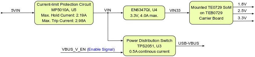
Figure 3: Board power distribution diagram.
Power Rails
| Module Connector (B2B) Designator | VCC / VCCIO | Direction | Pins | Notes |
|---|---|---|---|---|
| JB1 | VIN33 | Out | Pin 1, 2, 3, 4, 5, 6 | 3.3V module supply voltage |
| VCCIO_13 | Out | Pin 101, 102 | PL IO-bank VCCIO | |
| VCCIO_33 | Out | Pin 29, 30 | PL IO-bank VCCIO | |
| 3.3V | In | Pin 65, 66 | voltage output from module | |
| JB2 | 1.8V | In | Pin 49 | voltage output from module |
| 2.5V | In | Pin 13 | voltage output from module | |
| USB-VBUS | Out | Pin 107 | USB Host supply voltage | |
| VBAT_IN | Out | Pin 118 | RTC buffer voltage |
Table 19: Power pin description of B2B Module Connector.
| Jumper / Header Designator | VCC / VCCIO | Direction | Pins | Notes |
|---|---|---|---|---|
| J6 | VCCIO_33 | Out | Pin 2, 4, 6 | - |
| 1.8V | In | 5 | - | |
| 2.5V | In | 3 | - | |
| 3.3V | In | 1 | - | |
| J7 | VCCIO_13 | Out | Pin 2, 4, 6 | - |
| 1.8V | In | 5 | - | |
| 2.5V | In | 3 | - | |
| 3.3V | In | 1 | - |
Table 20: Power Pin description of VCCIO selection jumper pin header.
| Main Power Jack and Pins Designator | VCC / VCCIO | Direction | Pins | Notes |
|---|---|---|---|---|
| J12 | 5VIN | In | - | - |
| J9 | 5VIN | In | Pin A1, A2 | '5VIN' power supply to the Carrier Board as alternative to J12 |
| J2 | VBAT_IN | In | Pin 1 | Attention: Pin 2 connected to ground. VBAT_IN voltage on this pin cause short-circuit. |
Table 21: Main Power jack and pins description.
| Peripheral Socket Designator | VCC / VCCIO | Direction | Pins | Notes |
|---|---|---|---|---|
| J10 / J11 | USB-VBUS | Out | Pin 1 | USB2.0 Type A socket / Micro USB2.0 B socket |
| J1 | VIN33 | Out | Pin 4 | MikroSD Card socket VDD |
Table 22: Power pin description of peripheral connector.
| XMOD Header Designator | VCC / VCCIO | Direction | Pins | Notes |
|---|---|---|---|---|
| JB3 | 3.3V | - | Pin 5 | not connected |
| VIO | Out | Pin 6 | connected to VIN33 |
Table 23: Power pin description of XMOD/JTAG Connector.
Board to Board Connectors
Unable to render {include} The included page could not be found.
Variants Currently In Production
| Module Variant | Operating Temperature | USB Socket | Temperature Range |
|---|---|---|---|
| TEB0729-02-A | -40°C to +125°C | USB2.0 Type A socket fitted | Industrial |
| TEB0729-02-B | -40°C to +125°C | Micro USB2.0 B socket fitted | Industrial |
Table 24: Module variants.
Technical Specifications
Absolute Maximum Ratings
Parameter | Min | Max | Units | Reference Document |
|---|---|---|---|---|
5VIN supply voltage | -0.3 | 7 | V | MP5010A, EN6347QI data sheet |
Storage temperature | -65 | 150 | °C | - |
Table 25: Module absolute maximum ratings.
Recommended Operating Conditions
| Parameter | Min | Max | Units | Reference Document |
|---|---|---|---|---|
| 5VIN supply voltage | 4.75 | 5.25 | V | USB2.0 specification concerning 'VBUS' voltage |
| Operating temperature | -40 | 125 | °C | - |
Table 26: Module recommended operating conditions.
Operating Temperature Ranges
Industrial grade: -40°C to +85°C.
The TEB0729 Carrier Board itself is capable to be operated at industrial grade temperature range.
Please check the operating temperature range of the mounted SoM, which determine the relevant operating temperature range of the overall system.
Physical Dimensions
Board size: 107.70 mm × 100 mm. Please download the assembly diagram for exact numbers.
Mating height with standard connectors: 8 mm.
PCB thickness: ca. 1.65mm.
Highest part on the PCB is the Ethernet RJ-45 jack, which has an approximately 17 mm overall height. Please download the step model for exact numbers.
All dimensions are given in millimeters.
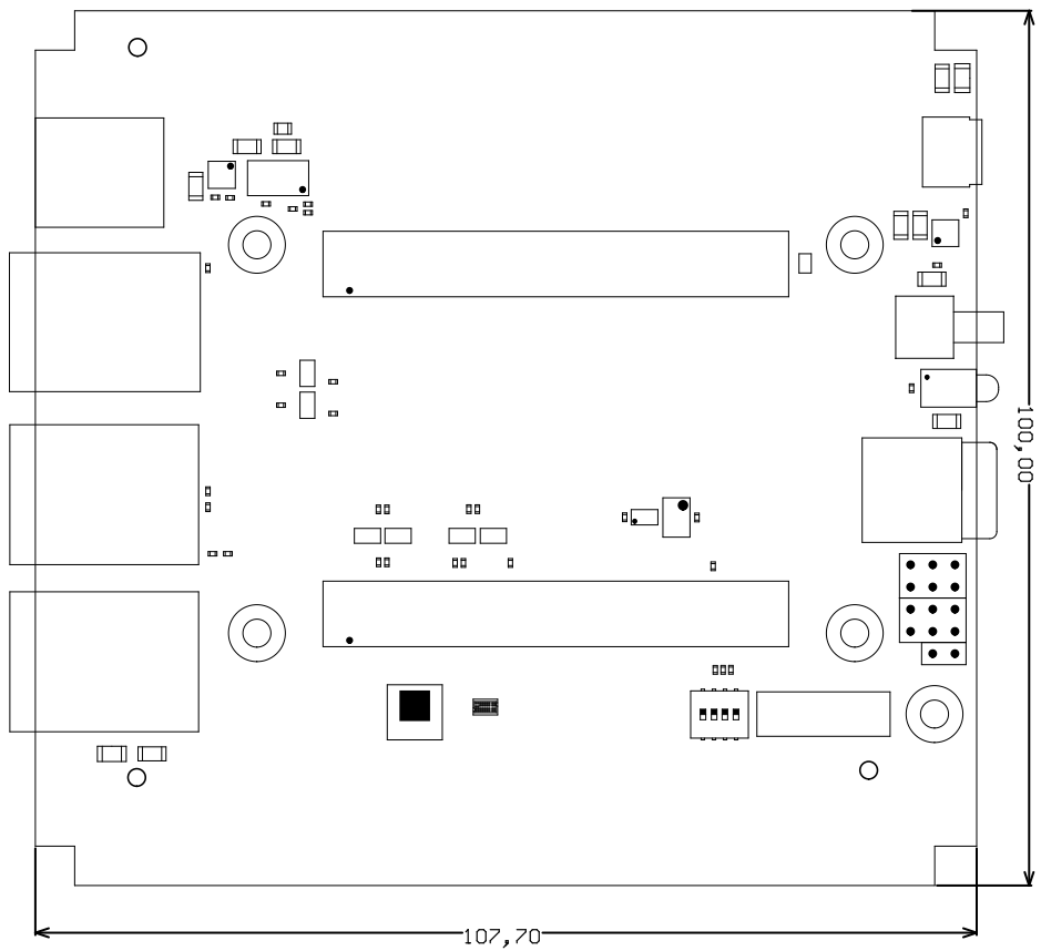
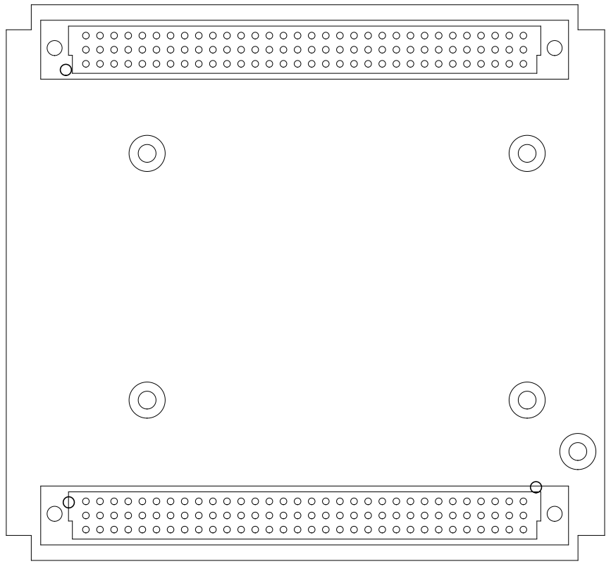
Figure 4: Board physical dimensions drawing.
Revision History
Hardware Revision History
| Date | Revision | Notes | PCN | Schematic Change Notes | Documentation Link | Note |
|---|---|---|---|---|---|---|
| - | 01 | First Production Release | - | - | TEB0729-01 | - |
| - | 02 | Second Production Release | - | Refer to Changes list in Schematic | TEB0729-02 | HW-Modification since 22.08.2017 |
Table 27: Module hardware revision history.
Hardware revision number can be found on the PCB board together with the module model number separated by the dash.
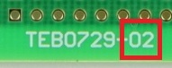
Figure 5: Module hardware revision number.
Document Change History
Date | Revision | Contributors | Description |
|---|---|---|---|
| Ali Naseri | initial document |
Table 28: Document change history.
Disclaimer
Data Privacy
Please also note our data protection declaration at https://www.trenz-electronic.de/en/Data-protection-Privacy
Document Warranty
The material contained in this document is provided “as is” and is subject to being changed at any time without notice. Trenz Electronic does not warrant the accuracy and completeness of the materials in this document. Further, to the maximum extent permitted by applicable law, Trenz Electronic disclaims all warranties, either express or implied, with regard to this document and any information contained herein, including but not limited to the implied warranties of merchantability, fitness for a particular purpose or non infringement of intellectual property. Trenz Electronic shall not be liable for errors or for incidental or consequential damages in connection with the furnishing, use, or performance of this document or of any information contained herein.
Limitation of Liability
In no event will Trenz Electronic, its suppliers, or other third parties mentioned in this document be liable for any damages whatsoever (including, without limitation, those resulting from lost profits, lost data or business interruption) arising out of the use, inability to use, or the results of use of this document, any documents linked to this document, or the materials or information contained at any or all such documents. If your use of the materials or information from this document results in the need for servicing, repair or correction of equipment or data, you assume all costs thereof.
Copyright Notice
No part of this manual may be reproduced in any form or by any means (including electronic storage and retrieval or translation into a foreign language) without prior agreement and written consent from Trenz Electronic.
Technology Licenses
The hardware / firmware / software described in this document are furnished under a license and may be used /modified / copied only in accordance with the terms of such license.
Environmental Protection
To confront directly with the responsibility toward the environment, the global community and eventually also oneself. Such a resolution should be integral part not only of everybody's life. Also enterprises shall be conscious of their social responsibility and contribute to the preservation of our common living space. That is why Trenz Electronic invests in the protection of our Environment.
REACH, RoHS and WEEE
REACH
Trenz Electronic is a manufacturer and a distributor of electronic products. It is therefore a so called downstream user in the sense of REACH. The products we supply to you are solely non-chemical products (goods). Moreover and under normal and reasonably foreseeable circumstances of application, the goods supplied to you shall not release any substance. For that, Trenz Electronic is obliged to neither register nor to provide safety data sheet. According to present knowledge and to best of our knowledge, no SVHC (Substances of Very High Concern) on the Candidate List are contained in our products. Furthermore, we will immediately and unsolicited inform our customers in compliance with REACH - Article 33 if any substance present in our goods (above a concentration of 0,1 % weight by weight) will be classified as SVHC by the European Chemicals Agency (ECHA).
RoHS
Trenz Electronic GmbH herewith declares that all its products are developed, manufactured and distributed RoHS compliant.
WEEE
Information for users within the European Union in accordance with Directive 2002/96/EC of the European Parliament and of the Council of 27 January 2003 on waste electrical and electronic equipment (WEEE).
Users of electrical and electronic equipment in private households are required not to dispose of waste electrical and electronic equipment as unsorted municipal waste and to collect such waste electrical and electronic equipment separately. By the 13 August 2005, Member States shall have ensured that systems are set up allowing final holders and distributors to return waste electrical and electronic equipment at least free of charge. Member States shall ensure the availability and accessibility of the necessary collection facilities. Separate collection is the precondition to ensure specific treatment and recycling of waste electrical and electronic equipment and is necessary to achieve the chosen level of protection of human health and the environment in the European Union. Consumers have to actively contribute to the success of such collection and the return of waste electrical and electronic equipment. Presence of hazardous substances in electrical and electronic equipment results in potential effects on the environment and human health. The symbol consisting of the crossed-out wheeled bin indicates separate collection for waste electrical and electronic equipment.
Trenz Electronic is registered under WEEE-Reg.-Nr. DE97922676.
Overview
Content Tools