<!--
Template Revision 1.68
(HTML comments will be not displayed in the document, no need to remove them. For Template/Skeleton changes, increase Template Revision number. So we can check faster, if the TRM style is up to date).
-->
HTML
<!--
General Notes:
If some section is CPLD firmware dependent, make a note and if available link to the CPLD firmware description. It's in the TE shop download area in the corresponding module -> revision -> firmware folder.
-->
HTML
<!--
General Notes:
Designate all graphics and pictures with a number and a description. For example "Figure 1: TE07xx-xx Block Diagram" or "Table 1: Initial delivery state". "Figure x" and "Table x" have to be formatted to bold.
-->
HTML
<!--
Link to the base folder of the module (remove de/ or en/ from the URL): for example:
https://shop.trenz-electronic.de/Download/?path=Trenz_Electronic/Modules_and_Module_Carriers/4x5/4x5_Carriers/TE0703/
  -->
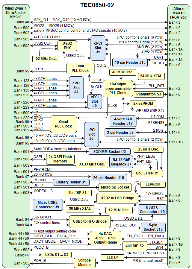
The Trenz Electronic TEC0850 is an industrial-grade MPSoC SoM integrating a Xilinx Zynq UltraScale+ MPSoC, with 64-bit wide SODIMM DDR4 SDRAM, max. Dual 512 MByte Flash memory for configuration and operation. 24 Gigabit transceivers on PL side and 4 PS side. Powerful switch-mode power supplies for all onboard voltages. A large number of configurable I/Os. 3U form factor.
HTML
<!--
Use short link the Wiki resource page: for example:
http://trenz.org/tef1001-info
List of available short links: https://wiki.trenz-electronic.de/display/CON/Redirects
  -->
Scroll Only (inline)
Refer to http://trenz.org/tec0850-info for the current online version of this manual and other available documentation.
Key Features
...
Block Diagram
HTML
<!--
Rules for all diagrams:
1. All diagrams are wrapped in the "Scroll Title" macro.
	- The title has to be named with the diagrams name
	- The anchor has the designation figure_x, whereby x is the number of the diagram

2. The Draw.IO diagram has to be inserted in the "Scroll Ignore" macro
	- Border has to be switched off in the macro edit
	- Toolbar has to be hidden in the macro edit

3. A PNG Export of the diagram has to be inserted in the "Scroll Only" macro, see Wiki page "Diagram Drawing Guidelines" how to do this step.

The workaround with the additional PNG of the diagram is necessary until the bug of the Scroll PDF Exporter, which cuts diagram to two pages, is fixed.


IMPORTANT NOTE: In case of copy and paste the TRM skeleton to a new Wiki page, delete the Draw.IO diagrams and the PNGs, otherwise due to the linkage of the copied diagrams every change in the TRM Skeleton will effect also in the created TRM and vice versa!

See page "Diagram Drawing Guidelines" how to clone an existing diagram as suitable template for the new diagram!

   -->
Scroll Title
anchor
Figure_1
title
Figure 1: TEC0850-02 block diagram
Scroll Ignore
draw.io Diagram
border
true
viewerToolbar
true
fitWindow
false
diagramName
TEC0850 overview
simpleViewer
false
width
diagramWidth
641
revision
1
Scroll Only
Main Components
Scroll Title
anchor
Figure_2
title
Figure 2: TEC0850-02 main components
Scroll Ignore
Scroll Only
...
...
Initial Delivery State
Storage device name
Content
Notes
...
...
..
Boot Process
Signals, Interfaces and Pins
Scroll Title
anchor
Figure_2
title
Figure 2: TEC0850-02 Overview IO interfaces
Scroll Ignore
draw.io Diagram
border
false
viewerToolbar
true
fitWindow
false
diagramDisplayName
lbox
true
revision
9
diagramName
IO Diagram
simpleViewer
true
width
links
auto
tbstyle
top
diagramWidth
641
Scroll Only
USB-C
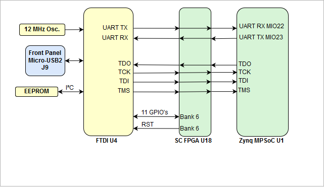
Front panel USB-C Interface connected to USB FIFO bridge chip FT601Q. 32-bit FIFO bridge provides a simple high-speed interface to Zynq UltraScale+ PL.
Front panel Micro-USB Interface provides access to UART and JTAG functions via FTDI FT2232 chip. Use of this feature requires that USB driver is installed on your host PC. UART0 with MIO 22 .. 23 should be selected in "Zynq UltraScale+ MPSoC" configuration.
The Digilent plug-in software and cable drivers must be installed on your machine for you to be able to use JTAG interface.
Scroll Title
anchor
Figure_3
title
Figure 3: JTAG/UART Interface
Scroll Ignore
draw.io Diagram
border
false
viewerToolbar
true
fitWindow
false
diagramDisplayName
lbox
true
revision
4
diagramName
uart_jtag
simpleViewer
true
width
links
auto
tbstyle
top
diagramWidth
641
Scroll Only
SD
There are some limitations to use SD card Interface in Linux.
Zynq UltraScale+ SD controller is working only in the 3.3V mode as it connected to SD card socket using 1.8V to 3.3V level shifter U10.
Micro SD card socket has no "Write Protect" switch.
Tip
To force Linux driver not to use this features add following instructions to device tree file.
&sdhci1 {
no-1-8-v; disable-wp; };
RJ45 -Ethernet
cPCIe
...
MGT
The TEC0850 board has 30 MGT lines routed to backplane connectors.
Bank
Connector
Lanes
PL 128
J4G and J4H
4
PL 129
J5A and J5B
4
PL 130
J5C and J5D
4
PL 230
J4G and J4H
4
PL 229
J5A and J5B
4
PL 228
J5C and J5D
4
PS 505
J1A
4
MGT reference clocks are connected to banks 129, 229 and 505. Banks 128 and 130 should share clock from bank 129, banks 230 and 228 from bank 229.
USB Interface
Zynq UltraScale+ USB controller connected to backplane connector J1C via USB PHY chip U11.
DDR4 SODIMM Socket
The Zynq UltraScale+ DDRC hard memory controller is wired to the DDR4 SODIMM Socket U3.
Circular Push Pull Connector
PicoBlade Connector
Pin Heater 2,54mm (2x5)
Battery holder
On-board Peripherals
Zynq UltraScale XCZU15EG MPSoC
The TEC0850 board is populated with the Zynq UltraScale+ XCZU15EG-1FFVB1156E MPSoC.
Main IO interfaces are shown on the image below.
PS MIO Configuration
MIO
Interface
MIO 0...12
QSPI Flash Memory
MIO 20...21
I2C 1
MIO 22...23
UART 0
MIO 26...37
GEM 0
MIO 46...51
SD 1
MIO 52...63
USB 0
MIO 64...75
USB 1
MIO 76...77
MDIO 0
Table 10: Default MIO Configuration
MAX10 System Controller
System controller chip is Intel MAX10 10M08SAU169C8G Chip with board control firmware.
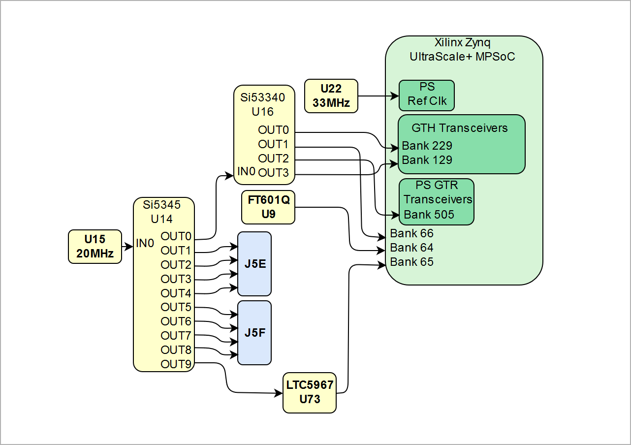
Programmable Clock Generators
Scroll Title
anchor
Figure_2
title
Figure 2: TEF1001-02 main components
Scroll Ignore
draw.io Diagram
border
false
viewerToolbar
true
fitWindow
false
diagramDisplayName
lbox
true
revision
3
diagramName
Clocks Diagram
simpleViewer
true
width
links
auto
tbstyle
top
diagramWidth
641
Scroll Only
I2C
The onboard I2C bus is connected to MIO 20...21 pins. Devices on the bus shown in the table below.
I2C address
Chip
Description
0x69
U14 Si5345
Clock generator and distributor
Oscillators
FTDIs
FT2232H
FT601Q-B-T
Quad-SPI Flash Memory
Board has two N25Q512A11G1240E connected in a dual parallel mode.
EEPROMs
I2C
The onboard I2C bus is connected to MIO 20...21 pins. Devices on the bus shown in the table below.
I2C address
Chip
Description
0x50
U63 24AA128T-I/ST
128K Serial EEPROM
0x53
U64 24AA025E48T-I/OT
2K Serial EEPROM with EUI-48™ or EUI-64™ Node Identity
USB PHY
Gigabit Ethernet PHY
Board has Marvell Alaska 88E1512 Ethernet PHY which use MDIO address 1.
8Bit DACs
Board has 4 8-bit parallel Texas Instruments THS5641 DACs with up to 100 MSPS Update Rate.
<!--
If power sequencing and distribution is not so much, you can join both sub sections together
  -->
Anchor
power_supply
power_supply
Power Consumption
The maximum power consumption of a module mainly depends on the design running on the FPGA.
Xilinx provide a power estimator excel sheets to calculate power consumption. It's also possible to evaluate the power consumption of the developed design with Vivado. See also Trenz Electronic Wiki FAQ.
Power Input
Typical Current
TBD*
Table : Typical power consumption.
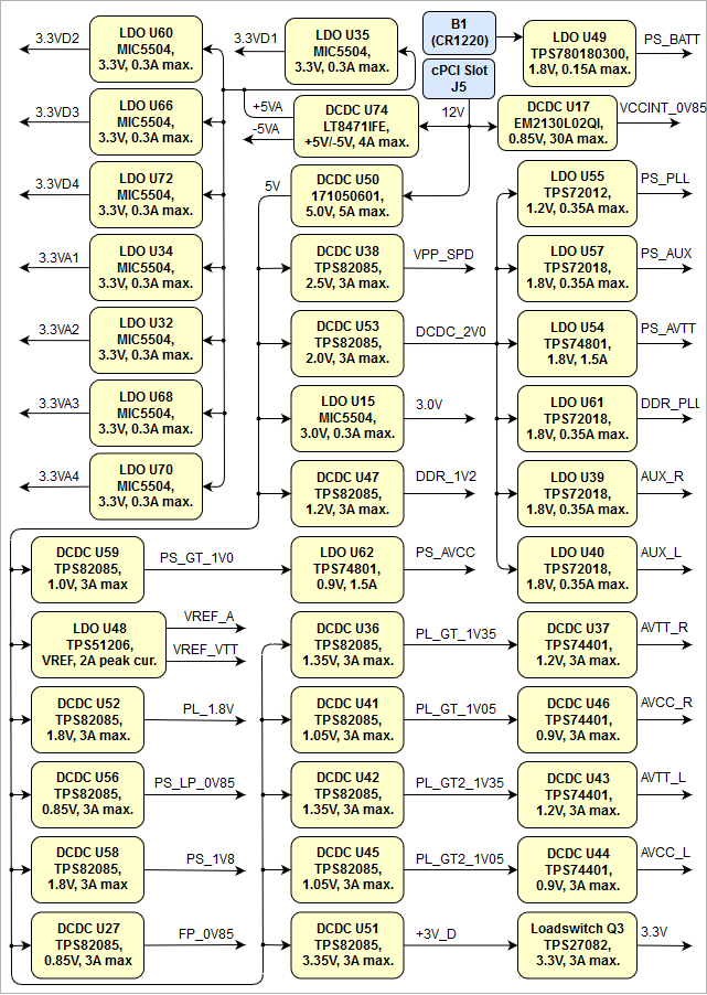
Power Distribution Dependencies
Scroll Title
anchor
Figure_3
title
Figure 3: Power Distribution
Scroll Ignore
draw.io Diagram
border
false
viewerToolbar
true
fitWindow
false
diagramDisplayName
lbox
true
revision
3
diagramName
Power supply
simpleViewer
true
width
links
auto
tbstyle
top
diagramWidth
642
Scroll Only
Power-On Sequence
Power Rails
Bank Voltages
Variants Currently In Production
HTML
<!--
Set correct link to the overview table of the product on english and german, if not available, set
https://shop.trenz-electronic.de/de/Produkte/Trenz-Electronic/
https://shop.trenz-electronic.de/en/Products/Trenz-Electronic/
  -->
Hardware revision number can be found on the PCB board together with the module model number separated by the dash.
Scroll Title
anchor
Figure_6
title
Figure 6: Module hardware revision number
Document Change History
HTML
<!--
Generate new entry:
1.add new row below first
2.Copy "Page Information Macro(date)" Macro-Preview, Metadata Version number, Author Name and description to the empty row. Important Revision number must be the same as the Wiki document revision number
3.Update Metadata = "Page Information Macro (current-version)" Preview+1 and add Author and change description.
  -->