...
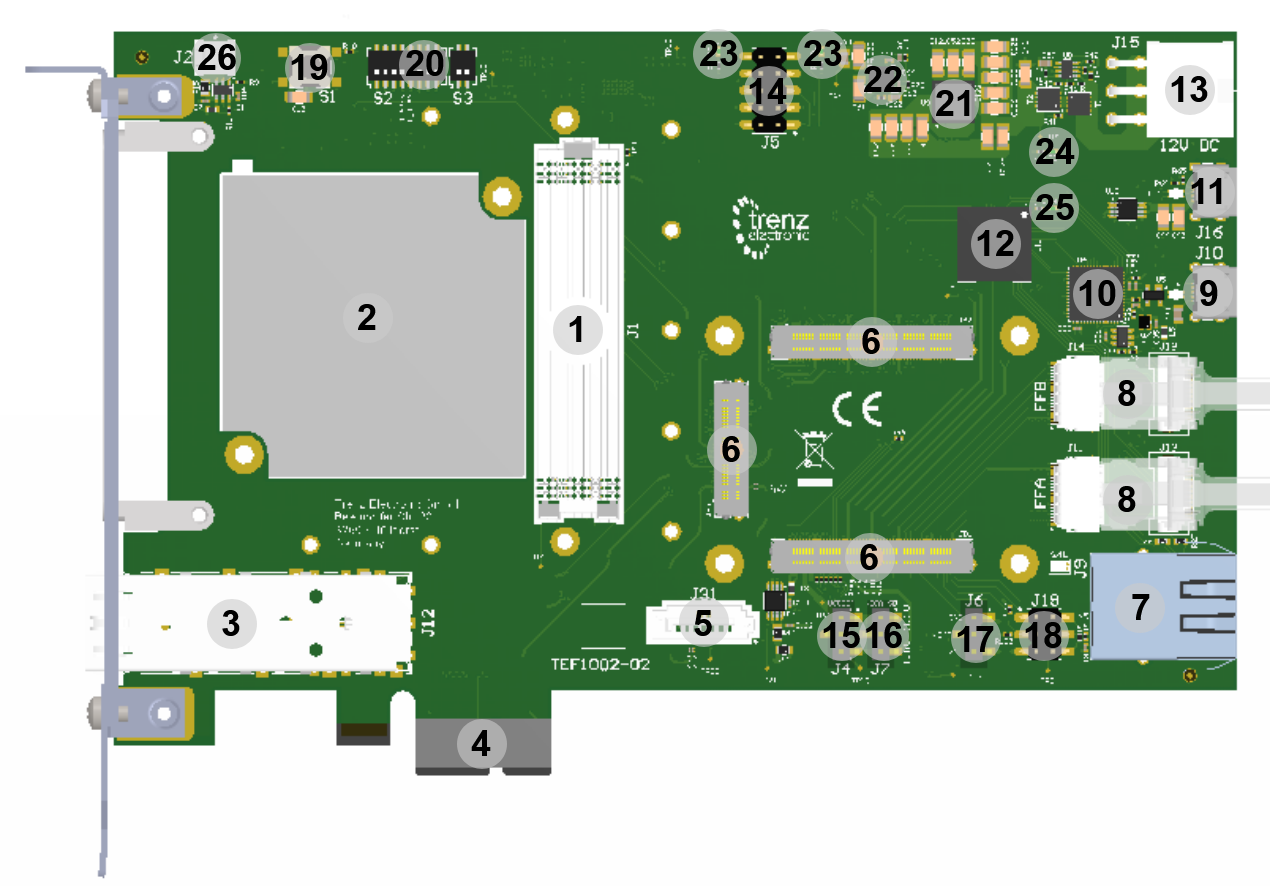
Carrier for 4x5 modules
LPC FMC
- SFP+ connector
- PCIe x1
- SATA connector
- RJ45 Gigabit Ethernet connector
- micro-usb to JTAG/UART bridge
- 2x Firefly high speed LVDS connectors
- micro usb connector
- micro SD card connector
- 4x LED (2User, Power and Status)
- Module reset button
- 10x user dip
MAX10 CPLD
...
| Scroll Title |
|---|
| anchor | Figure_OV_MC |
|---|
| title | TE... main components |
|---|
|
| Scroll Ignore |
|---|
| draw.io Diagram |
|---|
| border | false |
|---|
| viewerToolbar | true |
|---|
| |
|---|
| fitWindow | false |
|---|
| diagramDisplayName | |
|---|
| lbox | true |
|---|
| revision | 45 |
|---|
| diagramName | TE1002-01_Main_components_top |
|---|
| simpleViewer | false |
|---|
| width | |
|---|
| links | auto |
|---|
| tbstyle | top |
|---|
| diagramWidth | 638641 |
|---|
|
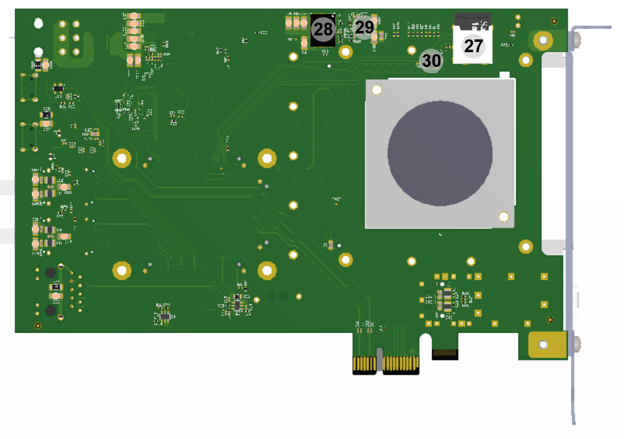
| draw.io Diagram |
|---|
| border | true |
|---|
| viewerToolbar | true |
|---|
| |
|---|
| fitWindow | false |
|---|
| diagramName | TE1002-01_Main_components_bottom |
|---|
| simpleViewer | false |
|---|
| width | |
|---|
| diagramWidth | 635 |
|---|
| revision | 4 |
|---|
|
|
| Scroll Only |
|---|
|
|
- ANSI/VITA 57.1 compliant FMC LPC connector, J1
- Cooling fan 5VDC M1 (45X5MM, 0.7W, 1.06CFM), M1
- SFP+ connector, J12
- PCIe x1 connector, J3
- SATA connector, J31
- Trenz Electronic 4 x 5 modules B2B connectors, JB1 ... JB3
- RJ45 Gigabit Ethernet connector, J9
- 2x Firefly high speed LVDS arrangement of connectors , J11, J13, J14, J18
- Micro-USB2 connector, J10
- FTDI FT2232H USB2 to JTAG,UART/FIFO Bridge, U4
- Micro-USB2 connector, J16
- MAX10 10M08SAU169C8G CPLD, U11
- 6-pin 12V power connector, J15
- 6x1 JTAG pin header (not fitted)
- 3x1 jumper pin header (select VCCIOA), J4
- 3x1 jumper pin header (select VCCA_SD), J7
- 2x1 pin header (VBAT), J6
- 2x5 1,27mm pitch pin header (PJTAG), J19
- Push button, S1
- 10x dip switch, S2, S3
- DCDC LMZ23605TZ @5.0V (5V0PER), U15
- DCDC LMZ23605TZ @5.0V (5V0), U9
- DCDC LMZ23605TZ @3.3V(3V3IN), U10
- 2x green LED (user), D1, D2
- green LED (Power), D3
- green LED (Status), D4
- SD-Card connector (top loader),
- DCDC EN5335QI (FMC_VADJ), U1
- DCDC EN6338QI @3.3V (3V3FMC), U14
- SDIO Level shifter TXS02612, U3
...
| Scroll Title |
|---|
| anchor | Table_OV_CS |
|---|
| title | TEF1002 Control Signals |
|---|
|
| Scroll Table Layout |
|---|
| orientation | portrait |
|---|
| sortDirection | ASC |
|---|
| repeatTableHeaders | default |
|---|
| style | |
|---|
| widths | |
|---|
| sortByColumn | 1 |
|---|
| sortEnabled | false |
|---|
| cellHighlighting | true |
|---|
|
Control signal | Switch / Button / LED / Pin | Signal Schematic Names | Connected to | Functionality | Notes |
|---|
| FMC_VADJ voltage selection | DIP switches S2-1, S2-2, S2-3 | VID0 ... VID2 | SC CPLD U11, pins K6, J5, K5 | sets adjustable voltage for FMC connector | dependens on SC CPLD configuration | | JTAG enable | DIP switch S2-4 | JTAGEN | SC CPLD U11, pin E5 | OFF: TEF1002 SC CPLD JTAG enabled,
ON: Module/FMC JTAG enabled | - | | Module JTAG select | DIP switch S2-5 | M_JTAGEN | B2B JB1, pin 90 | When S2-4 ON and S2-6 OFF: OFF: Module SC CPLD JTAG enabled, ON: Module SOC JTAG enabled | - | | FMC JTAG select | DIP switch S2-6 | FMC_JTAG | SC CPLD U11,L3 | When S2-4 ON: OFF: TEF1002 SC CPLD JTAG enabled, ON: FMC JTAG enabled | dependens depends on SC CPLD configuration, only avialiable when 4x5 module installed | | Enable module power | DIP switch S2-7 | CM0 | SC CPLD U11, M3 | Module power. Set ON to enable module power. (Power management depends on module. ) | dependens depends on SC CPLD configuration, only avialiable when 4x5 module installed | | No sequenzing | DIP switch S2-8 | CM1 | SC CPLD U11, L2 | Module Power management. Set ON to disable module CPLD power management. Power management depends on module and not all modules support extended power management with CPLD. | dependens depends on SC CPLD configuration, only avialiable when 4x5 module installed | | Boot Mode | DIP switch S3-1 | CM2 | SC CPLD U11, K2 | Boot Mode for attached module (Default: OFF for primary SD boot and ON for primary QSPI boot. Depends also on module CPLD firmware). | dependens depends on SC CPLD configuration, only avialiable when 4x5 module installed | | FMC VADJ enable | DIP switch S3-2 | USR0 | SC CPLD U11, K1 | ON: FMC VADJ enable also without installed FMC Card OFF: FMC_FADJ only enabled when FMC installed. | dependens on SC CPLD configuration, only avialiable when 4x5 module installed | | Reset | Push button S1 | BUTTON | SC CPLD U11, N6 | Module Reset, Low active module reset. Pin force Power one reset on FPGA/SoC. | dependens depends on SC CPLD configuration | | 2x User LED | Green LEDs D1, D2 | LED1, LED2 | SC CPLD U11, J5, K5 | Depends on User configuration, curenntly both off, if not otherwise programmed. | dependens depends on SC CPLD configuration | | Board power indicator | Green LED D3 | 3V3IN | B2B JB1, pin 14, 16 | ON: 3.3V on-board voltage available | - | | Board status indicators | Green LED D4 | - | SC CPLD U11, pin C2 | ON: No failure. For other blinking status of this LED please refer to SC Firmware description. | dependens on SC CPLD configuration | | Enable module power | SC CPLD U11, D11 | EN1 | B2B JB1, pin 27 | Module power. (Power management depends on module. ) | - | | No sequenzing | SC CPLD U11, E13 | NOSEQ | B2B JB1, pin 8 | Power management depends on module and not all modules support extended power management with CPLD. | - | | Boot Mode | SC CPLD U11, B11 | MODE | B2B JB1, pin 31 | Boot Mode for attached module. LOW for primary SD boot and HIGH for primary QSPI boot. (Depends also on module CPLD firmware). | - | | Module Reset | SC CPLD U11, E12 | RESIN | B2B JB2, pin 17 | Module Reset | - |
|
...
| Scroll Title |
|---|
| anchor | Table_SIP_B2B |
|---|
| title | General overview of PL I/O signals and SoM's interfaces connected to the B2B connectors |
|---|
|
| Scroll Table Layout |
|---|
| orientation | portrait |
|---|
| sortDirection | ASC |
|---|
| repeatTableHeaders | default |
|---|
| style | |
|---|
| widths | |
|---|
| sortByColumn | 1 |
|---|
| sortEnabled | false |
|---|
| cellHighlighting | true |
|---|
|
| B2B Connector | Interfaces | I/O Signal Count | Notes |
|---|
| JB1 | User IO | 15 single ended or 7 differential | TEF1002 CPLD |
|
| 16 single ended or 8 differential | FFA |
|
| 16 single ended or 8 differential | FFB |
| MIO/PJTAG/User IO | 4 | Pinheader J19 |
| CPLD IO | 2 | Module CPLD IO to Carrier CPLD |
| SD IO | 6 | - |
| UART | 2 | - |
| GbE PHY_MDIO + PHY_COM | 8 +1 | - |
| Module Control | 5 | NOSEQ,, EN1, PGOOD, MODE, M_JTAGEN | JB2 | User IO | 12 single ended or 6 differential | LPC FMC |
| MGTs (RX+TX) | 4 | PCIe x1, SFP+, LPC FMC, SATA |
| MGTCLK | 1 differential | - |
| CLK | 1 differential | - |
| USB | 2 | OTG-D_P, OTG-D_N |
| USB Control | 3 | OTG-ID | | JB3 | User IO | 56 single ended or 28 differential | LPC FMC |
| CLK | 2 differential | M2C |
| JTAG | 4 | - |
|
...
| Scroll Title |
|---|
| anchor | Table_SIP_FMC |
|---|
| title | FMC connector interface |
|---|
|
| Scroll Table Layout |
|---|
| orientation | portrait |
|---|
| sortDirection | ASC |
|---|
| repeatTableHeaders | default |
|---|
| style | |
|---|
| widths | |
|---|
| sortByColumn | 1 |
|---|
| sortEnabled | false |
|---|
| cellHighlighting | true |
|---|
|
| FMC Connector J2 Pins and Interfaces | I/O Signal Count | LVDS-pairs count | Connected to | VCCIO voltage | Notes |
|---|
| I/O | 56 | 28 | B2B JB2 connector | FMC_VADJ | pins usable as single ended I/O's or LVDS pairs | | 12 | 6 | B2B JB3 connector | FMC_VADJ | | Multi Gigabit Transceiver | - | 2 | B2B JB3 connector, pin 19, 21 and 20, 22 | - | RX, TX | | Gigabit Transceiver Clock | - | 1 | B2B JB3 connector, pin 31, 33 | - |
| | I²C (SDA, SCL) | 2 | - | SC CPLD U11, pin F9, J8 |
-| 3V3IN | FMC I²C Geographical Address pins GA0 and GA1 set to GND. | | JTAG |
4 M7, 3.3V | - | | , M7, N8 | 3V3IN | TDO, TMS, TCK, TDI, TRST | | Clock Input |
Clock Input-| FMC_VADJ | 2x reference clock inputs | | Control Signals | 2 | - | SC CPLD U11, pin M5, E9 |
-| 3V3IN | 'PG_C2M', 'FMC_PRSNT' | | Reference voltage (FMC_VREF) | - | - | - | - | Not Connected. |
|
SFP+ Interface
| Scroll Title |
|---|
| anchor | Table_SIP_FMCSFP |
|---|
| title | FMC connector SFP+ interface |
|---|
|
| Scroll Table Layout |
|---|
| orientation | portrait |
|---|
| sortDirection | ASC |
|---|
| repeatTableHeaders | default |
|---|
| style | |
|---|
| widths | |
|---|
| sortByColumn | 1 |
|---|
| sortEnabled | false |
|---|
| cellHighlighting | true |
|---|
|
| Connector J12 Pins and Interfaces | I/O Signal Count | LVDS-pairs count | Connected to | VCCIO voltage | Notes |
|---|
| Multi Gigabit Transceiver | - | 2 | B2B JB3 connector, pin 13, 15 and 14, 16 | - | RX, TX | | Control | 6 |
| SC CPLD U11 | 3V3_PER3V3IN | TX_FAULT, TX_DIS, M-DEF0, RS0, RS1, LOS | | I²C (SDA, SCL) | 2 | - | SC CPLD U11, pin F9, J8 | -3V3IN | MUX via CPLD |
|
...
PCIe x1 card edge connector
| Scroll Title |
|---|
| anchor | Table_SIP_FMCPCIe |
|---|
| title | FMC PCIe x1 card edge connector interface |
|---|
|
| Scroll Table Layout |
|---|
| orientation | portrait |
|---|
| sortDirection | ASC |
|---|
| repeatTableHeaders | default |
|---|
| style | |
|---|
| widths | |
|---|
| sortByColumn | 1 |
|---|
| sortEnabled | false |
|---|
| cellHighlighting | true |
|---|
|
| Connector J12 J3 Pins and Interfaces | I/O Signal Count | LVDS-pairs count | Connected to | VCCIO voltage | Notes |
|---|
| Multi Gigabit Transceiver | - | 2 | B2B JB3 connector, pin 7, 9 and 8, 10 | - | RX, TX | | Gigabit Transceiver Clock | - | 1 | B2B JB3 connector, pin 32, 34 | - | I²C (SDA, SCL) | 2
| | JTAG | 5 | - | SC CPLD U11 | , pin F9, J8- | FMC I²C Geographical Address pins GA0 and GA1 set to GND. | | JTAG | 4 | - | SC CPLD U11, pin M7, N7, M8, F8 | 3.3V | - | | Clock Input | - | 2 | B2B JB3 connector | - | 2x reference clock inputs | | Control Signals | 2 | - | SC CPLD U11, pin M5, E9 | - | 'PG_C2M', 'FMC_PRSNT' | | Reference voltage (FMC_VREF) | - | - | - | - | Not Connected. |
|
microUSB JTAG/UART/FIFO Interface
The microUSB connector provides JTAG access through the carriers USB to JTAG/UART/FIFO bridge. JTAG is routed for MUX and CPLD JTAG access to the CPLD. UART signals are connected to the module B2B connectors. For further description of the JTAG MUX see Dip switches or SC CPLD Firmware. For non-standard functionalitiers compare on-board Peripherals and datasheet of FTDI FT2232H.
microUSB
RJ45 - Ethernet
On-board Peripherals
| Page properties |
|---|
|
Notes : - add subsection for every component which is important for design, for example:
- Ethernet PHY
- USB PHY
- Programmable Clock Generator
- Oscillators
- eMMCs
- RTC
- FTDI
- ...
- DIP-Switches
- Buttons
- LEDs
|
...
| , M12, M13, L11, N12, G10 | 3V3IN | TDO, TMS, TCK, TDI, TRST |
|
SATA connector
| Scroll Title |
|---|
| anchor | Table_SIP_SATA |
|---|
| title | SATA connector |
|---|
|
| Scroll Table Layout |
|---|
| orientation | portrait |
|---|
| sortDirection | ASC |
|---|
| repeatTableHeaders | default |
|---|
| style | |
|---|
| widths | |
|---|
| sortByColumn | 1 |
|---|
| sortEnabled | false |
|---|
| cellHighlighting | true |
|---|
|
| Connector J31 Pins and Interfaces | I/O Signal Count | LVDS-pairs count | Connected to | VCCIO voltage | Notes |
|---|
| Multi Gigabit Transceiver | - | 2 | B2B JB3 connector, pin 7, 9 and 8, 10 | - | RX, TX |
|
LVDS high speed connectors FFA and FFB
There are two connector arrangements mechanical compatible to Firefly connectors, but with high speed LVDS signals.
| Scroll Title |
|---|
| anchor | Table_SIP_FMC |
|---|
| title | FMC connector interface |
|---|
|
| Scroll Table Layout |
|---|
| orientation | portrait |
|---|
| sortDirection | ASC |
|---|
| repeatTableHeaders | default |
|---|
| style | |
|---|
| widths | |
|---|
| sortByColumn | 1 |
|---|
| sortEnabled | false |
|---|
| cellHighlighting | true |
|---|
|
| Connector, Pins and Interfaces | I/O Signal Count | LVDS-pairs count | Connected to | VCCIO voltage | Notes |
|---|
| FFA, J11 | - | 8 | B2B JB1 connector | - | - | | FFA Control, J14 | 4 | - | SC CPLD U11, pin C10, C9, E8, B9 | 3V3IN | MPRS, MSEL, INTL, RSTL | | FFA I2C, J14 | 2 | - | SC CPLD U11, pin E6, D6 | 3V3IN |
| | FFB, J11 | - | 8 | B2B JB1 connector | - | - | | FFB Control, J14 | 4 | - | SC CPLD U11, pin A11, B10, A10, B9 | 3V3IN | MPRS, MSEL, INTL, RSTL | | FFB I2C, J14 | 2 | - | SC CPLD U11, pin A9, D8 | 3V3IN |
|
|
The RSTL of both connectors are tied together.
microUSB JTAG/UART/FIFO Interface
The microUSB connector provides JTAG access through the carriers USB to JTAG/UART/FIFO bridge. JTAG is routed for MUX and CPLD JTAG access to the CPLD. UART signals are connected to the module B2B connectors. For further description of the JTAG MUX see Dip switches or SC CPLD Firmware. For non-standard functionalitiers compare on-board Peripherals and datasheet of FTDI FT2232H.
microUSB
| Scroll Title |
|---|
| anchor | Table_SIP_USB |
|---|
| title | MicroUSB J16 |
|---|
|
| Scroll Table Layout |
|---|
| orientation | portrait |
|---|
| sortDirection | ASC |
|---|
| repeatTableHeaders | default |
|---|
| style | |
|---|
| widths | |
|---|
| sortByColumn | 1 |
|---|
| sortEnabled | false |
|---|
| cellHighlighting | true |
|---|
|
| Connector J16, Pins and Interfaces | I/O Signal Count | LVDS-pairs count | Connected to | VCCIO voltage | Notes |
|---|
| DATA | - | 1 | B2B JB3 connector, pin 48, 50 | - | - | | Power, Control | 3 | - | B2B JB3 pin 52, 54, 56 | - | OTG-ID, VBUS_V_EN, USB-VBUS |
|
RJ45 - Ethernet MagJack
| Scroll Title |
|---|
| anchor | Table_SIP_ETH |
|---|
| title | Gigabit Ethernet Connector |
|---|
|
| Scroll Table Layout |
|---|
| orientation | portrait |
|---|
| sortDirection | ASC |
|---|
| repeatTableHeaders | default |
|---|
| style | |
|---|
| widths | |
|---|
| sortByColumn | 1 |
|---|
| sortEnabled | false |
|---|
| cellHighlighting | true |
|---|
|
| Connector J9, Pins and Interfaces | I/O Signal Count | LVDS-pairs count | Connected to | VCCIO voltage | Notes |
|---|
| PHY_MDI | - | 4 | B2B JB1 connector, pin 3, 5, 9, 11, 15, 17, 21, 23 | - | - | | LED1 | 2 | - | SC CPLD U11, pin B13, C12 | 3V3IN | green/yellow | | LED2 | 2 |
| SC CPLD U11, pin D12, C13 | 3V3IN | green/yellow |
|
micro SD-Card connector
The micro SD-Card connector J8 is connected to a TXS02612 SDIO port expander, which is used as levelshifter. Depending on the modules IO Voltage of the IO Bank where the SD-Card is connected Jumper J7 has to be set.
| Scroll Title |
|---|
| anchor | Table_SIP_SDC |
|---|
| title | micro SD-Card connector |
|---|
|
| Scroll Table Layout |
|---|
| orientation | portrait |
|---|
| sortDirection | ASC |
|---|
| repeatTableHeaders | default |
|---|
| style | |
|---|
| widths | |
|---|
| sortByColumn | 1 |
|---|
| sortEnabled | false |
|---|
| cellHighlighting | true |
|---|
|
| Connector J8 pin | Signal Schematic Name
| Muxed to signal on Port Expander | Connected to | Notes |
|---|
| 2, DAT3 | SD-D3_LS | SD_D3 | B2B JB1, pin 18 | - | 3, CMD | SD-CMD_LS | SD_CMD | B2B JB1, pin 26 | - | 5, CLK | SD-CCLK_LS | SD_CCLK | B2B JB1, pin 28 | - | 7, DAT0 | SD-D0_LS | SD_D0 | B2B JB1, pin 24 | - | 8, DAT1 | SD-D1_LS | SD_D1 | B2B JB1, pin 22 | - | 1, DAT2 | SD-D2_LS | SD_D2 | B2B JB1, pin 20 | - |
|
On-board Peripherals
| Page properties |
|---|
|
Notes : - add subsection for every component which is important for design, for example:
- Ethernet PHY
- USB PHY
- Programmable Clock Generator
- Oscillators
- eMMCs
- RTC
- FTDI
- ...
- DIP-Switches
- Buttons
- LEDs
|
System Controller CPLD MAX10
The Intel/Altera MAX10 10M08SAU169C8G System Controller CPLD (U11) is the central system management unit where essential control signals are logically linked by the implemented logic in CPLD firmware. It generates output signals to control the system, the on-board peripherals and the interfaces. The JTAG and I2C between the on-board peripherals and the attached module are by-passed, forwarded and controlled by the System Controller CPLD. A main tasks of the System Controller CPLD is the monitoring of the power-on sequence and configuring the state of the attached module. For detailed information, refer to the firmware documentation of the SC CPLD. Table below lists the SC CPLD I/O signals and pins:
| Scroll Title |
|---|
| anchor | Table_SIP_CPLD |
|---|
| title | SC CPLD pin mapping |
|---|
|
| Scroll Table Layout |
|---|
| orientation | portrait |
|---|
| sortDirection | ASC |
|---|
| repeatTableHeaders | default |
|---|
| style | |
|---|
| widths | |
|---|
| sortByColumn | 1 |
|---|
| sortEnabled | false |
|---|
| cellHighlighting | true |
|---|
|
| Signal name | SC CPLD Pin | Connected to | Function | Notes |
|---|
| ACBUS0 | A4 | FTDI U4, pin 22 | GPIO's available to user
| (FIFO or other FTDI functions when FTDI reprogrammed)
| | ACBUS1 | B4 | FTDI U4, pin 23 | | ACBUS2 | A5 | FTDI U4, pin 24 | | ACBUS3 | B5 | FTDI U4, pin 25 | | ACBUS4 | A6 | FTDI U4, pin 26 | | ACBUS5 | B6 | FTDI U4, pin 27 | | ACBUS6 | A7 | FTDI U4, pin 28 | | ACBUS7 | A8 | FTDI U4, pin 29 | | ADBUS4 | A2 | FTDI U4, pin 17 | | ADBUS5 | B2 | FTDI U4, pin 18 | | ADBUS6 | A3 | FTDI U4, pin 19 | | ADBUS7 | B3 | FTDI U4, pin 20 | | TCK | G2 | FTDI U4, pin 12 | Forwarded JTAG signals from FTDI chip.
| (FIFO or other FTDI functions when FTDI reprogrammed)
| | TDI | F5 | FTDI U4, pin 13 | | TDO | F6 | FTDI U4, pin 14 | | TMS | G1 | FTDI U4, pin 15 | | M_TCK | H5 | JB2, pin 100 | 4x5 Module JTAG
| Bank with VCCIO is VREF_JTAG from Module
| | M_TDI | J2 | JB2, pin 96 | | M_TDO | J1 | JB2, pin 98 | | M_TMS | H6 | JB2, pin 94 | | FMC_TCK | F8 | J1, pin D29 | FMC JTAG
| TRST not used
| | FMC_TDI | M7 | J1, pin D30 | | FMC_TDO | N7 | J1, pin D31 | | FMC_TMS | M8 | J1, pin D33 | | FMC_TRST | N8 | J1, pin D34 | | PCIE_TCK | L11 | J3, pin A5 | PCIe JTAG
| Currently not used
| | PCIE_TDI | N12 | J3, pin A6 | | PCIE_TDO | M12 | J3, pin A7 | | PCIE_TMS | M13 | J3, pin A8 | | PCIE_TRST | G10 | J3, pin B9 | | PCIE_PERST | F12 | J3, pin A11 | Indication that PCIe Bus is up (power, clocks) |
| | EN_FMC | L4 | U14, pin 9 | Enable switched 3.3V FMC power | pulled down | | EN_FMC_VADJ | K7 | U1, pin 41 | Enable IO power FMC_VADJ | pulled down | | EN_PER | F13 | Q4, pin 5 | Enable perepherie power 3V3_PER | pulled down | | FAN_FMC_EN | K8 | Q1, pin 5 | Enable FMC FAN |
| | FMC_PG_C2M | M5 | J1, pin D1 | I | pulled up | | FMC_PRSNT_M2C_L | E9 | J1, pin H2 | Indicate if FMC installed | Low when FMC present | | FMC_SCL | J8 | J1, pin C31 | 2-wire serial bus |
| | FMC_SDA | F9 | J1, pin C30 |
|
| | PG_FMC_VADJ | J6 |
|
|
| | FF_RSTL | B9 |
|
| | FFA_INTL | E8 |
|
| | FFA_MPRS | C10 |
|
|
| | FFA_MSEL | C9 |
|
|
| | FFA_SCL | D6 |
|
|
| | FFA_SDA | E6 |
|
|
| | FFB_INTL | A10 |
|
|
| | FFB_MPRS | A11 |
|
|
| | FFB_MSEL | B10 |
|
|
| | FFB_SCL | D8 |
|
|
| | FFB_SDA | A9 |
|
|
| | CPLD_IO_1 | B12 |
|
|
| | CPLD_IO_2 | A12 |
|
|
| | M10_RST | D1 |
|
|
| | M10_RX | E4 |
|
|
| | M10_TX | E3 |
|
|
| | EN1 | D11 |
|
|
| | MODE | B11 |
|
|
| | NOSEQ | E13 |
|
|
| | PGOOD | C11 |
|
|
| | RESIN | E12 |
|
|
| | M3.3VOUT | M4 |
|
|
| | SFPA_LOS | M10 |
|
|
| | SFPA_M-DEF0 | F10 |
|
|
| | SFPA_RS0 | N10 |
|
|
| | SFPA_RS1 | M11 |
|
|
| | SFPA_SCL | L10 |
|
|
| | SFPA_SDA | N9 |
|
|
| | SFPA_TX_DIS | M9 |
|
|
| | SFPA_TX_FAULT | G9 |
|
|
| | VID0_FMC_VADJ | E10 |
|
|
| | VID1_FMC_VADJ | J7 |
|
|
| | VID2_FMC_VADJ | L5 |
|
|
| | VID0 | K6 |
|
|
| | VID1 | N5 |
|
|
| | VID2 | N4 |
|
|
| | JTAGEN | E5 |
|
|
| | FMC_JTAG | L3 |
|
|
| | CM0 | M3 |
|
|
| | CM1 | L2 |
|
|
| | CM2 | K2 |
|
|
| | USR0 | K1 |
|
|
| | USB_OC | D9 |
|
|
| | BUTTON | N6 |
|
|
| | LED1 | J5 |
|
|
| | LED2 | K5 |
|
|
| | PHY_LED1 | D12 |
|
|
| | PHY_LED1R | C13 |
|
| | PHY_LED2 | B13 |
|
| | PHY_LED2R | C12 |
|
| | A_00_N | J10 |
|
|
| | A_00_P | K10 |
| | A_01_N | L12 |
| | A_01_P | K11 |
| | A_02_N | J12 |
| | A_02_P | K12 |
| | A_03_N | H10 |
| | A_03_P | J9 |
| | A_04_N | H13 |
| | A_04_P | J13 |
| | A_05_N | H8 |
| | A_05_P | H9 |
| | A_06_N | G12 |
| | A_06_P | G13 |
| | A_07 | L13 |
|
|
FTDI FT2232H
SDIO Port Expander
Configuration DIP-switches
Jumper
Push Button
On-board LEDs
Power and Power-On Sequence
...