Table of Contents
Overview
The Trenz Electronic TEBF0808 carrier board is a baseboard for the Xilinx Zynq Ultrascale+ MPSoC modules TE0808 and TE0803, which exposes the module's B2B connector pins to accessible connectors and provides a whole range of on-board components to test and evaluate the Zynq Ultrascale+ SoMs and for developing purposes. The carrier board has a Mini-ITX form factor making it capable to be fitted into a PC enclosure. On the PC enclosure's rear and front panel, MGT interfaces and connectors are accessible, for the front panel elements there also Intel-PC compatible headers available.
Key Features
- Mini-ITX form factor, PC enclosure compatible
- ATX-24 power supply connector
- Optional 12V standard power plug
- Headers
- Intel 10-pin HDA Audio
- Intel 9-pin Power-/Reset-Button, Power-/HD-LED
- PC-BEEPER
- On-board Power- / Reset-Switches
- 2x Configuration 4-bit DIP-switches
- 2x Optional 4-wire PWM fan connectors
- PCIe Slot - one PCIe lane (16 lane connector)
- CAN FD Transceiver (10 Pin IDC connector and 6-pin header)
- 4x On-board configuration EEPROMs (1x Microchip 24LC128-I/ST, 3x Microchip 24AA025E48T-I/OT)
- Dual SFP+ Connector (2x1 Cage)
- 1x DisplayPort (single lane)
- 1x SATA Connector
- 2x USB3.0 A Connector (Superspeed Host Port (Highspeed at USB2.0))
- 1x USB3.0 on-board connector with two ports
- FMC HPC Slot (FMC_VADJ max. VCCIO)
- FMC Fan
- Gigabit Ethernet RGMII PHY with RJ45 MegJack
- All carrier board peripherals' I²C interfaces muxed to MPSoC's I²C interface
- Quad programmable PLL clock generator SI5338A
- 2x SMA coaxial connectors for clock signals
- MicroSD- / MMC-Card Socket (bootable)
- 32 Gbit (4 GByte) on-board eMMC flash (8 banks a 4 Gbit)
- 2x System Controller CPLDs Lattice MachXO2 1200 HC
- 1x Samtec FireFly (4 GT lanes bidirectional)
- 1x Samtec FireFly connector for reverse loopback
- 2x JTAG/UART header ('XMOD FTDI JTAG Adapter'-compatible) for programming MPSoC and SC CPLDs
- 20-pin ARM JTAG Connector (PS JTAG0)
- 3x PMOD connector (GPIO's and I²C interface to SC CPLDs and MPSoC module)
- On-board DC-DC PowerSoCs
Additional assembly options are available for cost or performance optimization upon request.
Block Diagram
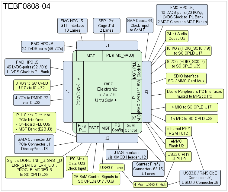
Figure 1: TEBF0808-04 Block Diagram
Main Components
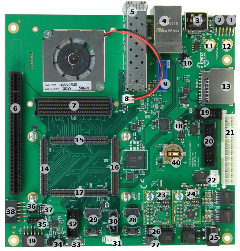
Figure 2: TEBF0808-04 Carrier Board
- PMOD connector, P2
- MicroSD Card socket (on bottom side), J16
- DisplayPort connector, J13
- USB3.0 A 2x , RJ45 1x (stacked), J7
- SFP+ 2x1 cage, J14
- PCIe x16 connector (one PCIe lane connected), J11
- FMC HPC connector, J5
- FMC-Fan connector 5V, J19
- USB3.0 connector, J8
- PC-BEEPER 4-pin header, J23
- SMA coaxial connector (SI5338A clock output), J32
- SMA coaxial connector (clock input to MPSoC module), J33
- MMC Card socket, J27
- Ultra fine 0.50 mm pitch, Razor Beam™ LP Slim Terminal Strip with 160 contacts, J4
- Ultra fine 0.50 mm pitch, Razor Beam™ LP Slim Terminal Strip with 160 contacts, J1
- Ultra fine 0.50 mm pitch, Razor Beam™ LP Slim Terminal Strip with 160 contacts, J3
- Ultra fine 0.50 mm pitch, Razor Beam™ LP Slim Terminal Strip with 160 contacts, J2
- CAN bus 6-pin header, J29
- CAN bus 10-pin connector, J24
- ARM JTAG 20-pin connector, J30
- ATX-24 power supply connector, J20
- 4-Wire PWM fan connector, J35
- JTAG/UART header ('XMOD FTDI JTAG Adapter'-compatible) for access to MPSoC module, J12
- JTAG/UART header ('XMOD FTDI JTAG Adapter'-compatible) for access to System Controller CPLDs, J28
- Power Jack 2.1mm 12V, J25
- 4-bit DIP-switch, S5
- Power Button, S1
- Samtec FireFly connector for reverse loopback, J21/J22
- Samtec FireFly connector (4 GT lanes bidirectional), J6/J15
- SATA header, J31
- 4-Wire PWM fan connector, J26
- I²C interface of programmable on-module PLL (10-pin header), J17
- Reset Button, S2
- INTEL HDA 9-pin header, J9
- Intel front panel (PWR-/RST-Button, HD-/PWR-LED) 9-pin header, J10
- Samtec FireFly connector J6/J15 I²C interface (3-pin header), J34
- 4-bit DIP-switch, S4
- PMOD connector, P3
- PMOD connector, P1
- Battery Holder CR1220, B1
Initial Delivery State
Storage device name | Content | Notes |
|---|---|---|
User configuration EEPROMs (1x Microchip 24LC128-I/ST, 3x Microchip 24AA025E48T-I/OT) | Not programmed | - |
| USB3.0 HUB Configuration EEPROM (Microchip 24LC128-I/ST) | Not programmed | - |
| Si5338A programmable PLL NVM OTP | Not programmed | - |
Table 1: Initial Delivery State of the flash memories
Signals, Interfaces and Pins
FMC HPC Connector
The FMC (FPGA Mezzanine Card) connector J5 with high pin count (HPC) provides as an ANSI/VITA 57.1 standard a modular interface to the MPSoCs FPGA and exposes numerous of its I/O pins for use by other mezzanine modules and expansion cards.
The connector supports single ended (VCCIO: FMC_VADJ) and differential signaling as the I/O's are routed from the FPGA banks as LVDS-pairs to the FMC connector.
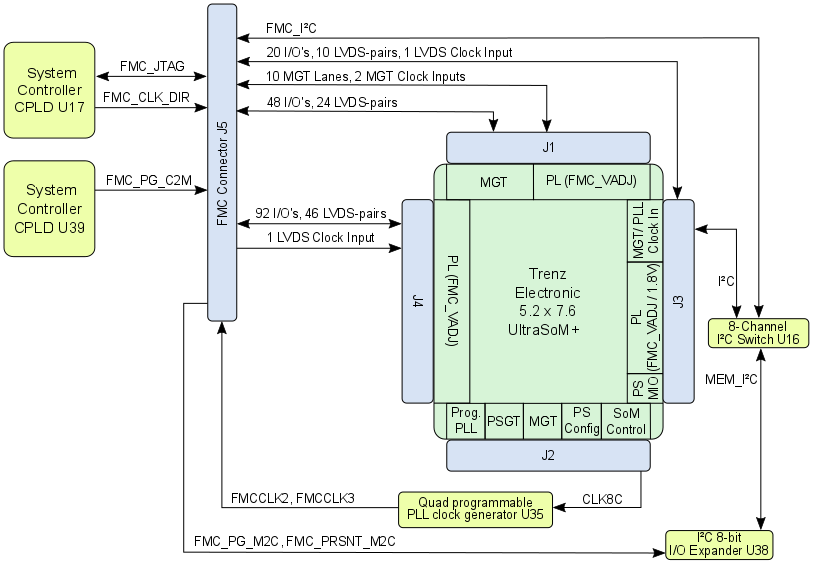
Figure 3: FMC HPC Connector
| FPGA Bank | I/O Signal Count | LVDS-pairs count | VCCO bank Voltage | Reference Clock Input from FMC Connector | Notes |
|---|---|---|---|---|---|
| Bank 48 | 20 | 10 | FMC_VADJ | 1 reference clock signal from FMC connector | - |
| Bank 64 | 46 | 23 | FMC_VADJ | 1 reference clock signal from FMC connector | bank's VREF-pin connected to FMC connector pin J5-H1 (VREF_A_M2C) |
| Bank 65 | 46 | 23 | FMC_VADJ | - | bank's VREF-pin connected to FMC connector pin J5-H1 (VREF_A_M2C) |
| Bank 66 | 48 | 24 | FMC_VADJ | - | bank's VREF-pin connected to FMC connector pin J5-H1 (VREF_A_M2C) |
Table 2: FMC connector pin-outs of available logic banks of the MPSoC
The MGT-banks have also clock input-pins which are exposed to the FMC connector. Following MGT-lanes are available on the FMC connectors J5:
| MGT Bank | Type | Count of MGT Lanes | Schematic Names / Connector Pins | MGT Bank's Reference Clock Inputs from FMC Connector |
|---|---|---|---|---|
| 228 | GTH | 4 GTH lanes | B228_RX3_P, B228_RX3_N, pins J5-A10, J5-A11 B228_RX2_P, B228_RX2_N, pins J5-A6, J5-A7 B228_RX1_P, B228_RX1_N, pins J5-A2, J5-A3 B228_RX0_P, B228_RX0_N, pins J5-C6, J5-C7 | 1 reference clock signal (B228_CLK0) from FMC connector Si5345 CLK3 signal of SoM's prog. PLL routed on-module to bank's pins N8/N7 |
| 229 | GTH | 4 GTH lanes | B229_RX3_P, B229_RX3_N, pins J5-B12, J5-B13 B229_RX2_P, B229_RX2_N, pins J5-B16, J5-B17 B229_RX1_P, B229_RX1_N, pins J5-A18, J5-A19 B229_RX0_P, B229_RX0_N, pins J5-A14, J5-A15 | 1 reference clock signal (B229_CLK0) from FMC connector Si5345 CLK2 signal of SoM's prog. PLL routed on-module to bank's pins J8/J7 |
| 230 | GTH | 2 GTH lanes | B230_RX1_P, B230_RX1_N, pins J5-B4, J5-B5 B230_RX0_P, B230_RX0_N, pins J5-B8, J5-B9 | Si5345 CLK1 signal of SoM's prog. PLL routed on-module to bank's pins E8/E7 |
Table 3: FMC connector pin-outs of available MGT lanes of the MPSoC
The FMC connector provides pins for reference clock output to the Mezzanine module and clock input to PL banks of the MPSoC:
| Clock Signal Schematic Name | FMC Connector Pins | Direction | Clock Source | Notes |
|---|---|---|---|---|
| B228_CLK0 | J5-D4 / J5-D5 | in | FMC Connector J5 | clock signal to MGT bank 228 |
| B229_CLK0 | J5-B20 / J5-B21 | in | FMC Connector J5 | clock signal to MGT bank 229 |
| FMCCLK2 | J5-K4 / J5-K5 | out | Carrier Board PLL SI5338A U35, CLK2 | - |
| FMCCLK3 | J5-J2 / J5-J3 | out | Carrier Board PLL SI5338A U35, CLK3 | - |
| B64_L14_P / B64_L14_N | J5-H4 / J5-H5 | in | FMC Connector J5 | bank 64 clock capable input pins |
| B48_L6_P / B48_L6_N | J5-G2 / J5-G3 | in | FMC Connector J5 | bank 48 clock capable input pins |
Table 4: FMC connector pin-outs for reference clock output
The FMC connector provides further interfaces like JTAG and I²C interfaces:
| Interfaces | I/O Signal Count | Pin schematic Names / FMC Pins | Connected to | Notes |
|---|---|---|---|---|
| JTAG | 5 | FMC_TCK, pin J5-D29 FMC_TMS, pin J5-D33 FMC_TDI, pin J5-D30 FMC_TDO, pin J5- D31 | SC CPLD U17, bank 1 | VCCIO: 3V3SB TRST_L, pin J5-D34 pulled-up to 3V3_PER |
| I²C | 2 | FMC_SCL, pin J5-C30 FMC_SDA, pin J5-C31 | I²C Switch U16 | I²C-lines pulled-up to 3V3_PER |
| Control Lines | 4 | FMC_PRSNT_M2C, pin J5-H2 FMC_PG_C2M, pin J5-D1 (3V3_PER pull-up) FMC_PG_M2C, pin J5-F1 (3V3_PER pull-up) FMC_CLK_DIR, pin J5-B1 (pulled-down to GND) | I²C I/O Expander U38 SC CPLD U39, bank 0 I²C I/O Expander U38 SC CPLD U17, bank 1 | 'PG' = 'Power Good'-signal 'C2M' = carrier to (Mezzanine) module 'M2C' = (Mezzanine) module to carrier |
Table 5: FMC connector pin-outs of available interfaces to the System Controller CPLD
Several VCCIO voltages are available on the FMC connector to operate the I/O's on different voltage levels:
| VCCIO Schematic Name | FMC Connector J5 Pins | Notes |
|---|---|---|
| 12V | C35/C37 | extern 12V power supply |
| 3V3_PER | D32/D36/D38/D40/C39 | 3.3V peripheral supply voltage |
| FMC_VADJ | H40/G39/F40/E39 | adjustable FMC VCCIO voltage, supplied by DC-DC converter U8 |
Table 6: Available VCCIO voltages on FMC connector
MIO Bank Interfaces
The TEBF0808 carrier board provides several interfaces, which are configured on the MIO banks 500 .. 503 of the Zynq Ultrascale+ MPSoC.
Following table contains the assignment of the MIO pins to the configured interfaces:
| MIO | Configured as | System Controller CPLD | Notes |
|---|---|---|---|
| 0..12 | Dual QSPI | - | Dual Flash Memory on TE0808 SoM; Bootable |
| 13..23 | SD0: eMMC | - | eMMC Memory U2; Bootable |
| 24, 25 | - | CPLD (U39) MUXED | - |
| 26..29 | - | CPLD (U17 MUXED | Bootable JTAG (PJTAG0) |
| 30 | force reboot after FSBL-PLL config for PCIe | CPLD (U39) MUXED | - |
| 31 | PCIe reset | CPLD (U39) MUXED | - |
| 32 | - | CPLD (U39) MUXED | - |
| 33 | - | CPLD (U39) MUXED | - |
| 34..37 | - | CPLD (U39) MUXED | - |
| 38, 39 | I2C0 | - | - |
| 40 | forwarded to PWRLED_P / LED_P | CPLD (U39) MUXED | - |
| 41 | - | - | - |
| 42, 43 | UART0 | CPLD (U39) MUXED | - |
| 44 | SD_WP to FPGA | CPLD (U39) MUXED | - |
| 45..51 | SD1: SD | - | Bootable MikroSD / MMC Card |
| 52..63 | USB0 | - | - |
| 64..75 | GEM3 | - | Ethernet RGMII |
| 76, 77 | MDC / MDIO | - | Ethernet RGMII |
Table 7: MIO Assignment
Following interfaces are provided by the MIO bank of the Zynq Ultrascale+ MPSoC:
- 4x USB3.0 Superspeed ports (downward compatible to USB2.0 Highspeed)
- SDIO port with muxed MikroSD and MMC Card socket
- Gigabit Ethernet interface connected per RGMII
- eMMC interface
- Master I²C interface to on-board peripherals
The block-diagram below visualizes the interfaces of the MIO bank at the Zynq Ultrascale+ MPSoC and their associated on-board peripherals.
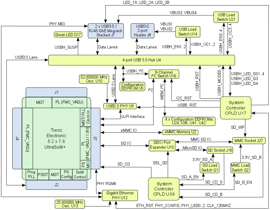
Figure 4: TEBF0808 MIO Interfaces
PS GT Bank 505 Interfaces
The PS GT Bank 505 provides beside the USB3.0 Lane also following interfaces:
- SATA (PS GT bank 505, MGT2 Lane)
- DisplayPort (PS GT bank 505, MGT3 Lane, only TX-pair routed)
- PCI Express (PS GT bank 505, MGT0 Lane)
| Function | MGT Lane | Required Ref Clock | Clock Source | Comment |
|---|---|---|---|---|
| PCIe | PS 0 | 100 MHz | Si5345 CLK0 signal of SoM's prog. PLL | clock signal routed on carrier board to PCIe connector J1 |
| USB3 | PS 1 | 100 MHz | Si5345 CLK4 signal of SoM's prog. PLL | clock signal routed on-module, |
| SATA | PS 2 | 150 MHz | On-board oscillator U23 | optional: Si5345 CLK4 signal of SoM's prog. PLL |
| DP.0 | PS 3 | 27 MHz | Si5345 CLK5 signal of SoM's prog. PLL | DisplayPort GT SERDES clock signal, Si5345 CLK6 signal of SoM's prog. PLL on-module routed to B128, |
Table 8: PS GT Lane Assignment
Following block diagram shows the wiring of the MGT Lanes of the PS GT bank 505 to the particular high speed data interfaces:
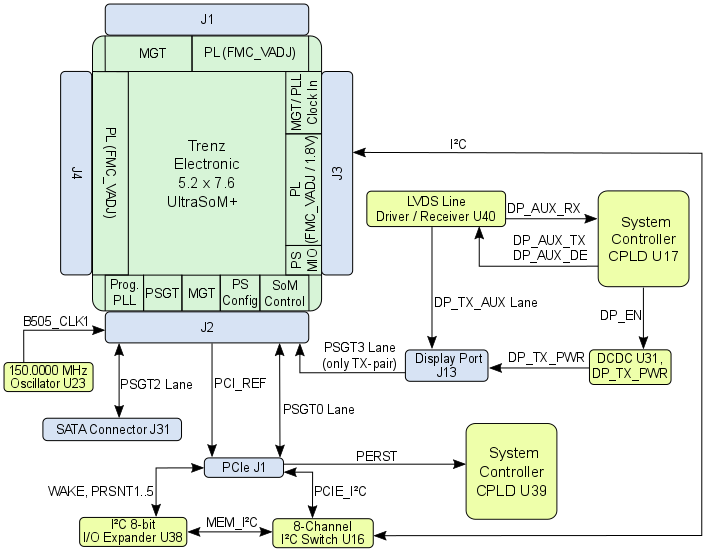
Figure 5: TEBF0808 PS GT Bank 505 Interface
MGT Interfaces SFP+ and FireFly
The TEBF0808 carrier board provides the high speed MGT interface connectors "SFP+" (Enhanced small form-factor pluggable) and Samtec "FireFly". Each of this connectors are capable of data transmission rates up to 10 Gbit/s.
| Function | MGT Lane | Required Ref Clock | Clock Source | Comment |
|---|---|---|---|---|
| FireFly | B128 MGT Lanes 0..3 | - | Si5345 CLK6 signal of SoM's prog. PLL | clock signal on-module routed to B128 |
| SFP | B230 MGT Lane 2 | 125 / 156.25 MHz | Si5345 CLK7 signal of SoM's prog. PLL | clock signal routed on carrier board to B230 |
| SFP | B230 MGT Lane 3 | 125 / 156.25 MHz | Si5345 CLK7 signal of SoM's prog. PLL | clock signal routed on carrier board to B230 |
Table 9: MGT Lane Assignment
Following block diagram show the wiring of the MGT lanes to the particular interface connectors:
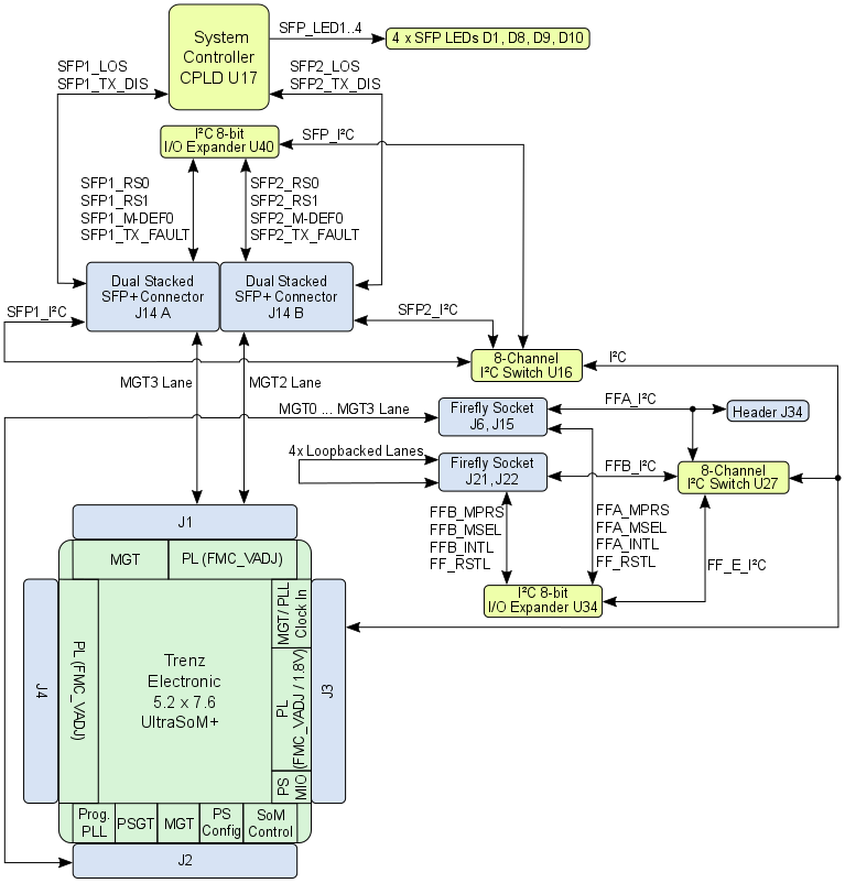
Figure 6: TEBF0808 MGT Interfaces
As shown on the block diagram, the FireFly connector pair J21, J22 provides four reversed looped back MGT lanes. To test any of the on-board MGT lanes or of an extern device, 4 RX/TX differential pairs are bridged on the connector, hence the transmitted data on these MGT lanes flows back to their sources in a loop-back circuit without intentional processing or modification.
CAN FD Interface and PMOD Connectors
On the carrier board there is a CAN FD (CAN with Flexible Data-Rate) interface available which is accessible on the CAN headers J24 (10-pin IDC connector) or J29 (6-pin header), which are connected to the CAN FD transceiver U30.
Additionally the carrier board provides PMOD connectors with GPIO and I²C interface:
| PMOD | Interface | Connected to | Notes |
|---|---|---|---|
| P1 | GPIO | HP Bank 65 of MPSoC (4 I/O's, B65_T0 ... B65_T3), System Controller CPLD U17 (4 I/O's, EX_IO1 ... EX_IO4) | Voltage translation via IC U33 with direction control, only singled-ended signaling possible |
| P2 | I²C | 8-channel I²C Switch U27 | Accessible on MPSoC's I²C interface through I²C switch U27 |
| P3 | I²C | 8-channel I²C Switch U27 | Accessible on MPSoC's I²C interface through I²C switch U27 |
Table 10: PMOD Pin Assignment
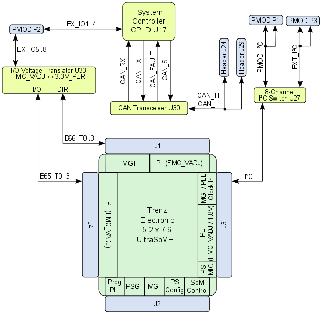
Figure 7: TEBF0808 CAN Interfaces, PMOD
Intel-PC Compatible Headers and FAN Connectors
The TEBF0808 carrier board provides with its Mini-ITX form factor the possibility to encase the boa rd in a PC Enclosure. For this purpose, the board is equipped with several Intel-PC compatible headers to connect them to the PC Enclosure.
Headers are available for following PC front panel elements
- Reset Button
- Power Button
- Power LED
- Hard Disc (HD) LED
- Intel High Definition Audio (HDA) Jacks
Following table gives an overview about the particular headers and a description about their functionalities:
| Header | Pin Name | Functionality | Connected to | Notes |
|---|---|---|---|---|
| J10 | Pin 1, HD LED+ | HD LED Anode | SC CPLD U39 | Reset and Power switch-pins are also connected to switch buttons S1 and S2 |
| J9 | Pin 1, PORT1L | Microphone Jack Left Microphone Jack Right Audio Out Jack Left Audio Out Jack Right Jack Detect / Mic in Ground | 24-bit Audio Codec U3 | - |
| J23 | Pin 1, 3V3SB Pin 4, S1 | 3.3V DC Supply PC compatible Beeper | SC CPLD U39 | - |
| J26 | Pin 1, GND | Ground 12V DC Supply RPM PWM | SC CPLD U39 | 4-wire PWM FAN connector |
| J35 | Pin 1, GND | Ground 12V DC Supply RPM PWM | SC CPLD U39 | 4-wire PWM FAN connector |
| J19 | Pin 1, GND | Ground 5V DC Supply | Load Switch Q3 (5V DC) | 2-wire FAN connector Fan off/on switchable by signal 'FAN_FMC_EN' on SC CPLD U39 |
Table 11: PC compatible Headers
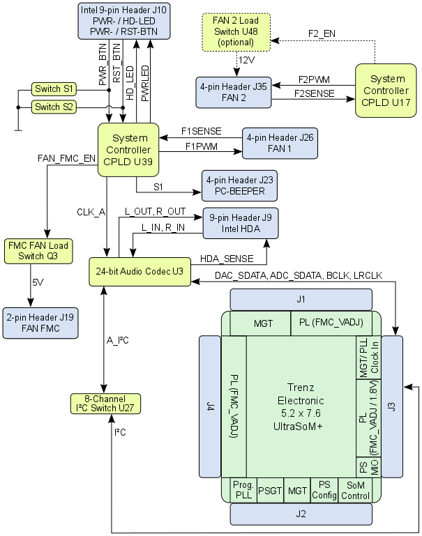
Figure 8: TEBF0808 PC Compatible Headers
JTAG Interface
The TEBF0808 carrier board provides several JTAG interfaces to program both the System Controller CPLDs and the Zynq Ultrascale+ MPSoC.
Therefore, the board is equipped with two JTAG/UART headers, which have 'XMOD FTDI JTAG Adapter'-compatible pin-assignment. So in use with the XMOD-FT2232H adapter-board TE0790 the mounted SoM and the System Controller CPLDs can be programmed via USB interface.
The System Controller CPLDs will be programmed by the XMOD-Header J28 in a cascaded JTAG chain as visualized in Figure 8. To program the System Controller CPLDs, the JTAG interface of these devices have to be activated by DIP-switch S4-3.
The 4 GPIO/UART pins (XMOD1_A/B/E/G) of the XMOD-Header J28 are routed to the System Controller CPLD U17.
XMOD-Header J12 is designated to program the Zynq Ultrascale+ MPSoC via USB interface, the 4 GPIO/UART pins (XMOD2_A/B/E/G) of this header are routed to the System Controller CPLD U39.
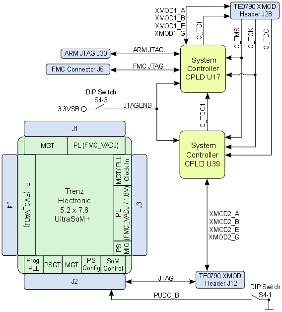
Figure 9: TEBF0808 JTAG interfaces
Further JTAG interfaces of the TEBF0808 carrier board are the ARM JTAG 20-pin IDC connector J30 and on the FMC Connector J5. This JTAG interfaces are connected to the System Controller CPLD U17, hence the logical processing and forwarding of the JTAG signals depend on the SC CPLD firmware. The documentation of the firmware of the SC CPLD U17 contains detailed information on this matter.
On-board Peripherals
System Controller CPDLs
The TEBF0808 is equipped with two System Controller CPLDs - Lattice Semiconductor LCMXO2-1200HC (MachXO2 Product Family) - with the schematic designators U17 and U39.
The SC-CPLD is the central system management unit where essential control signals are logically linked by the implemented logic of the CPLD firmware, which generates output signals to control the system, the on-board peripherals and the interfaces. Interfaces like JTAG and I2C between the on-board peripherals and to the FPGA-module are by-passed, forwarded and controlled by the System Controller CPLD.
Other tasks of the System Controller CPLD are the monitoring of the power-on sequence and to display the programming state of the FPGA module.
Both Sytem Controller CPLDs are connected to the Zynq Ultrascale+ MPSoC through MIO, PL IO-bank pins and I²C interface. The CPLDs are connected with each other through the IO pins SC_IO0 ... SC_IO8.
The functionalities and configuration of the pins depend on the CPLDs' firmware. The documentations of the firmware of SC CPLD U17 and SC CPLD U39 contains detailed information on this matter.
Following block diagram visualizes the connection of the SC CPLDs with the Zynq Ultrascale+ MPSoC via PS (MIO), PL bank pins and I²C interface.
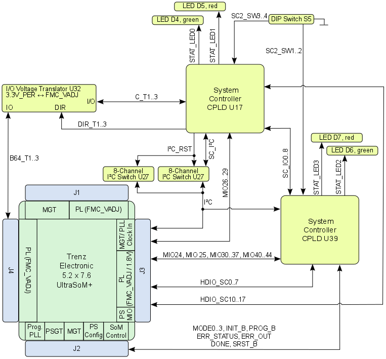
Figure 10: TEBF0808 System Controller CPLDs
Programmable PLL Clock Generator
The TEBF0808 Carrier Board is equipped with a Silicon Labs I2C programmable quad PLL clock generator Si5338A (U35). It's output frequencies can be programmed by using the I2C bus with address 0x70.
A 25 MHz (U7) oscillator is connected to pin 3 (IN3) and is used to generate the output clocks.
Once running, the frequency and other parameters can be changed by programming the device using the I2C-bus connected through I²C switch U16 between the Zynq module (master) and reference clock signal generator (slave).
| Si5338A (U35) Input | Signal Schematic Name | Note |
|---|---|---|
IN1/IN2 | CLK8_P, CLK8_N | Reference clock signal from Si5345 (CLK8 of prog. PLL on mounted SoM) |
IN3 | reference clock signal from oscillator SiTime SiT8008BI (U7) | 25.000000 MHz fixed frequency. |
IN4/IN6 | pins put to GND | LSB (pin 'IN4') of the default I²C-adress 0x70 not activated. |
IN5 | not connected | - |
| Si5338A (U35) Output | Signal Schematic Name | Note |
CLK0 A/B | SC_CLK0 | Reference clock signal to SC CPLD U17 (single-ended signaling) |
CLK1 A/B | SC_CLK1 | Reference clock signal to SC CPLD U17 (single-ended signaling) |
CLK2 A/B | FMCCLK2_P, FMCCLK2_N | Clock signal routed to FMC connector J5, pins J5-K4 / J5-K5 |
| CLK3 A/B | FMCCLK3_P, FMCCLK3_N | Clock signal routed to FMC connector J5, pins J5-J2 / J5-J3 |
Table 12: Pin description of PLL clock generator Si5338A
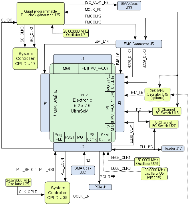
Figure 11: Clocking Configuration of TE0808 SoM on TEBF0808 Carrier Board
Si5338 OTP ROM is not programmed by default at delivery, so it is customers responsibility to either configure Si5338 during FSBL or then use SiLabs programmer and burn the OTP ROM with customer fixed clock setup.
Si5338 OTP can only be programmed two times, as different user configurations may required different setup, TEBF0808 is normally shipped with blank OTP.
For more information Si5338 at SiLabs.
Refer to the TE0808 TRM for the internal routing of the on-module Si5345 10-channel PLL clock generator signals to the clock input pins of the MGT banks.
Also how to configure the programmable Si5345 PLL clock generator on the mounted TE0808 SoM.
Oscillators
The TEBF0808 carrier board is equipped several on-board oscillators to provide the Zynq Ultrascale+ MPSoC's PS and PL banks and the on-board peripherals with reference clock-signals:
| Clock Source | Schematic Name | Frequency | Clock Input Destination |
|---|---|---|---|
| SiTime SiT8008BI oscillator, U10 | USB0_RCLK | 52.000000 MHz | USB 2.0 transceiver PHY U9, pin 26 |
| SiTime SiT8008BI oscillator, U13 | ETH_CLK | 25.000000 MHz | Gigabit Ethernet PHY U12, pin 34 |
| SiTime SiT8008BI oscillator, U7 | - | 25.000000 MHz | Quad PLL clock generator U35, pin 3 |
| DSC1123 oscillator, U23 | B505_CLK1 | 150.0000 MHz | PS GT Bank 505, dedicated for SATA interface |
DSC1123 oscillator, U6 optional, not equipped | B505_CLK0 | 100.0000 MHz | PS GT Bank 505, dedicated for USB interface |
Silicon Labs 570FBB000290DG, U45 optional, not equipped | B47_L5 (LVDS) | 250.MHz | HD Bank 47 clock capable input pins |
| SiTime SiT8008BI oscillator, U25 | CLK_CPLD | 25.576000 MHz | System Controller CPLD U35, pin 128 |
Table 13: Reference clock signal oscillators
High-speed USB ULPI PHY
USB PHY (U9) is provided by USB3320 from Microchip. The ULPI interface is connected to the Zynq Ultrascale+ PS USB0. I/O voltage is fixed at 1.8V and PHY reference clock input is supplied from the on-board 52.000000 MHz oscillator (U10).
| PHY Pin | Connected to | Notes |
|---|---|---|
| ULPI | PS bank MIO52 ... MIO63 | Zynq Ultrascale+ USB0 MIO pins are connected to the PHY |
| REFCLK | - | 52MHz from on board oscillator (U9) |
| REFSEL[0..2] | - | All pins set to GND selects the external reference clock frequency (52.000000 MHz) |
| RESETB | SC CPLD U17 | Low active USB PHY Reset (pulled-up to PS_1.8V). |
| DP, DM | 4-port USB3.0 Hub U4 | USB2.0 data lane |
| CPEN | - | External USB power switch active-high enable signal |
| VBUS | 5V | Connected to USB VBUS via a series of resistors, see schematic |
| ID | - | For an A-device connect to the ground. For a B-device, leave floating |
Table 14: USB PHY interface connections
Gigabit Ethernet PHY
On-board Gigabit Ethernet PHY (U12) is provided with Marvell Alaska 88E1512 IC. The Ethernet PHY RGMII interface is connected to the Zynq Ultrascale+ Ethernet0 PS GEM3. I/O voltage is fixed at 1.8V for HSTL signaling. The reference clock input of the PHY is supplied from the on-board 25.000000 MHz oscillator (U13). The 125MHz PHY output clock (PHY_CLK125M) is routed to System Controller CPLD U17, pin 70.
| PHY Pin | Connected to | Notes |
|---|---|---|
| MDC/MDIO | PS bank MIO76, MIO77 | - |
| PHY LED0..1 | SC CPLD U17, pin 67,86 | see schematic for details, forwarded to RJ45 GbE MagJack J7 |
| PHY_LED2 / INTn: | SC CPLD U17, pin 85 | Active low interrupt line |
| PHY_CLK125M | SC CPLD U17, pin 70 | 125 MHz Ethernet PHY clock out |
| CONFIG | SC CPLD U17, pin 65 | Permanent logic high |
| RESETn | SC CPLD U17, pin 62 | Active low reset line |
| RGMII | PS bank MIO64 ... MIO75 | Reduced Gigabit Media Independent Interface |
| SGMII | - | Serial Gigabit Media Independent Interface |
| MDI | RJ45 GbE MagJack J7 | Media Dependent Interface |
Table 15: Ethernet PHY interface connections
8-Channel I²C Switches
All on-board peripherals's interfaces and on-module peripherals with exposed I²C interface to B2B connectors are muxed to the I²C interface of the Zynq Ultrascale+ MPSoC as master.
For this purpose, the TEBF0808 carrier board is equipped with two 8-channel I²C switches provided by TCA9548A from Texas Instruments, together creating up to 16 switched I²C channels.
Refer to the data sheet of the TCA9548A chip how to address and and transmit data to the I²C slave devices through this switches.
The I2C bus works internally on-module with reference voltage 1.8V, it is connected to the PS I2C interface via PS MIO bank 501, pins MIO38 and MIO39, configured as master.
| MIO | Signal Schematic Name | Notes |
|---|---|---|
| 38 | I2C_SCL | 1.8V reference voltage |
| 39 | I2C_SDA | 1.8V reference voltage |
Table 16: MIO-pin assignment of the module's I2C interface
I2C addresses for on-board slave devices are listed in the table below:
| I²C Slave Devices | I²C Slave Address | Schematic Names of I²C Bus Lines | I²C Switch |
|---|---|---|---|
| 8-channel I²C switch U16 | 0x73 | I2C_SDA / I2C_SCL | - |
| 8-channel I²C switch U27 | 0x77 | I2C_SDA / I2C_SCL | - |
| On-module Quad programmable PLL clock generator Si5345 | 0x69 | PLL_SDA / PLL_SCL | U27 |
| Configuration EEPROM U24 | 0x54 | MEM_SDA / MEM_SCL | U16 |
| Configuration EEPROM U36 | 0x52 | MEM_SDA / MEM_SCL | U16 |
| Configuration EEPROM U41 | 0x51 | MEM_SDA / MEM_SCL | U16 |
| Configuration EEPROM U22 | 0x50 | MEM_SDA / MEM_SCL | U16 |
| 8-bit I²C IO Expander U44 | 0x26 | SFP_SDA / SFP_SCL | U16 |
| 24-bit Audio Codec U3 | 0x38 | A_I2C_SDA / A_I2C_SCL | U27 |
| USB3.0 Hub configuration EEPROM U5 | 0x51 | USBH_SDA / USBH_SCL | U16 |
| USB3.0 Hub | 0x60 | USBH_SDA / USBH_SCL | U16 |
| 8-bit I²C IO Expander U38 | 0x27 | MEM_SDA / MEM_SCL | U16 |
| On-board Quad programmable PLL clock generator U35 Si5338 | 0x70 | MCLK_SDA / MCLK_SCL | U16 |
| 8-bit I²C IO Expander U34 | 0x24 | FF_E_SDA / FF_E_SCL | U27 |
| SC CPLD U17, bank 3, pins 13 (SDA), 14 (SCL) | User programmable | SC_SDA / SC_SCL | U27 |
| SC CPLD U39, bank 2, pins 52 (SDA), 50 (SCL) | User programmable | I2C_SDA / I2C_SCL | - |
Table 17: On-board peripherals' I2C-interfaces device slave addresses
There are further I²C interfaces connected to the 8-channel I²C switches U16 and U27, which are provided by connectors with I²C interface. The I²C slave addresses depend on the devices, which are attached to this connectors:
| Connector | Schematic Names of I²C Bus Lines | I²C Switch |
|---|---|---|
| PCIe Connector J1 | PCIE_SDA / PCIE_SCL | U16 |
| SFP+ Connector J14A | SFP1_SDA / SFP1_SCL | U16 |
| SFP+ Connector J14B | SFP2_SDA / SFP2_SCL | U16 |
| FireFly Connector J15 | FFA_SDA / FFA_SCL | U27 |
| FireFly Connector J22 | FFB_SDA / FFB_SCL | U27 |
| FMC Connector J5 | FMC_SDA / FMC_SCL | U16 |
| PMOD Connector P1 | PMOD_SDA / PMOD_SCL | U27 |
| PMOD Connector P3 | EXT_SDA / EXT_SCL | U27 |
Table 18: On-board connectors' I2C-interfaces overview
Configuration EEPROMs
The TEBF0808 carrier board contains several EEPROMs for configuration and general user purposes. The EEPROMs are provided by Microchip and all have I²C interfaces:
| EEPROM Modell | Schematic Designator | Memory Density | Purpose |
|---|---|---|---|
| 24LC128-I/ST | U24 | 128 Kbit | user |
| 24AA025E48T-I/OT | U36 | 2 Kbit | user |
| 24AA025E48T-I/OT | U41 | 2 Kbit | user |
| 24AA025E48T-I/OT | U42 | 2 Kbit | user |
| 24LC128-I/ST | U5 | 128 Kbit | USB3.0 Hub U4 configuration memory |
Table 19: On-board configuration EEPROMs overview
4-port USB3.0 Hub
On the carrier board there are up to 4 USB3.0 Super Speed ports available, which are also downward compatible to USB2.0 High Speed ports. The USB3.0 ports are provided by Cypress Semiconductor CYUSB3324 4-port USB3.0 Hub controller U4. The pin-strap configuration option of the USB3.0 Hub is disabled, so this controller gets the configuration data and parameter from the configuration EEPROM U5. The I²C interface of the EEPROM and the controller is also accessible by the Zynq Ultrascale+ MPSoC through I²C switch U16.
On the Upstream-side, this controller is connected to the MGT1 lane of MPSoC's PS GT bank 505 to establish the USB3.0 data lane. For the USB2.0 interface, the controller is connected to the on-board USB2.0 PHY U9. The USB2.0 PHY is connected per ULPI interface (MIO pins 52..63) to MPSoC's MIO bank 501.
The USB3.0 Hub controller has also an ARM Cortex-M0 controller integrated, refer to the data sheet for further features and programmable options.
CAN FD Transceiver
On-board CAN FD (Flexible Data Rate) transceiver is provided by Texas Instruments TCAN337. This controller is the physical layer of the CAN interface and is specified for data rates up to 1 Mbps. The controller has many protection features included to ensure CAN network robustness and to eliminate the need for additional protection circuits. Refer to the data sheet of this transceiver for more details and specifications.
The transceiver is connected to System Controller CPLD U17, means it works on this interface with 3.3V VCCIO. The logical signal processing of the CAN interface depends on the current firmware ot the SC CPLD U17.
eMMC Memory
The TEBF0808 carrier board is equipped with embedded MMC memory connected to the PS MIO bank (MIO13 ... MIO23) of the Zynq Ultrascale+ MPSoC. The memory is provided by MTFC4GACAJCN-4M from Micron Technology. It has a memory density of 32 Gbit (4 GByte) and is sectored into 8 banks a 4 Gbit.
24-bit Audio Codec
For high resolution digital audio signal processing, the TEBF0808 carrier board is equipped with the Analog Devices 24-bit Audio Codec chip ADAU1761 with the schematic designator U3. The Audio Codec chip is connected to the Intel High Defintion Audio (Intel HDA) compatible 9-pin header J9 with single-ended signaling for analog stereo audio signal input and output. It supports also MIC / Jack detect. Its I²C control interface is accessible by the Zynq Ultrascale+ MPSoC through I²C switch U27.
The 24-bit Audio Codec provides numerous features and is also fully programmable with its dedicated graphical tool from the manufacturer. Refer to the data sheet of this chip for more detail information and specifications.
SDIO Port Expander
Due to the different signaling voltage levels of the MicroSD and MMC Card interfaces (3.3V) and the PS MIO bank of the Zynq Ultrascale+ MPSoC (1.8V), there is voltage-translation necessary, which is fullfilled by the SDIO port expander Texas Instruments TXS02612, U15. This IC also muxes the MikroSD and the MMC Card sockets to the SDIO port of the MPSoC, which is controlled by the signal 'SEL_SD' of the System Controller CPLD U39. The SC CPLD U39 also controls the load switches to enable the card sockets J16 and J27 and to report the card detect signal both of the sockets to the MPSoC (see schematic).
DIP-Switches
There are two 4 bit DIP Switches on the TEBF0808 carrier board to configure options and set parameters. The table below describes the functionalities of the particular switches:
| DIP-switch S4 | Position ON | Position OFF | Notes |
|---|---|---|---|
| S4-1 | PUDC_B is Low | PUDC_B is HIGH | Internal pull-up resistors during configuration are enabled at ON-position, means I/O's are 3-stated until configuration of the FPGA completes. |
| S4-2 | x | x | not connected |
| S4-3 | SC CPLDs' JTAG enabled | SC CPLDs' JTAG disabled | JTAG interface is enabled on both SC CPLDs, as this CPLDs are configured in a casdaced JTAG chain. |
| S4-4 | DC-DC converter U18 (5V) enabled | DC-DC converter U18 (5V) not manually enabled | In OFF-position, the DC-DC-converter will be still enabled by the Enable-signal of SC CDPD U17 (wired-OR circuit). |
Table 20: DIP-switch S4 functionality description
DIP-switch S5 located close to PWR push-button is connected to the two System Controller CPLDs, its functionalities depend on the current firmware of the CPLDs.
The switches of this DIP-switch have to be set in bit-patterns to set a parameter like boot mode or FMC_VADJ value:
| S5-1 | S5-2 | S5-3 | S5-4 | Description |
|---|---|---|---|---|
| ON | ON | ON | ON | Default, boot from SD/eMMC, 1.8V FMC VADJ |
| ON | ON | x | x | Boot from microSD, SD or SPI Flash |
| OFF | ON | x | x | Boot from eMMC |
| ON | OFF | x | x | Boot mode PJTAG0 |
| OFF | OFF | x | x | Boot mode main JTAG |
| x | x | x | ON | FMC VADJ = 1.8V |
| x | x | x | OFF | FMC VADJ = 1.2V |
Table 21: DIP-switch S4 functionality description
On-board LEDs
The TEBF0808 carrier board is equipped with several LED to signal current states and activities. The functionality of the LEDs D4 ... D7 depends on the current firmware of the SC CPLDs U17 and U39.
| LED | Color | Description and Notes |
|---|---|---|
| D4 | green | Status LED, connected to SC CPLD U17 |
| D5 | red | Status LED, connected to SC CPLD U17 |
| D6 | green | Status LED, connected to SC CPLD U39 |
| D7 | red | Status LED, connected to SC CPLD U39 |
| D1 | red | SFP+ interface status LED, connected to SC CPLD U17 |
| D8 | green | SFP+ interface status LED, connected to SC CPLD U17 |
| D9 | red | SFP+ interface status LED, connected to SC CPLD U17 |
| D10 | green | SFP+ interface status LED, connected to SC CPLD U17 |
| D17 | green | LED is on if all USB3.0 and USB 2.0 ports are in the suspend state and is |
Table 22: On-board LEDs functionality description
Power and Power-On Sequence
Power Consumption
The maximum power consumption of a module mainly depends on the design which is running on the FPGA.
Xilinx provide a power estimator excel sheets to calculate power consumption. It's also possible to evaluate the power consumption of the developed design with Vivado. See also Trenz Electronic Wiki FAQ.
Power Management
The TEBF0808 carrier board manages both the power-on sequence of the mounted TE0808 SoM and the on-board DC-DC converters via System Controller CPLD U39.
The power-on sequence of the TE0808 SoM is managed by utilizing the SoM's DC-DC converter control signals ('Enable', 'Power-Good'), so the DC-DC converters of the SoM dedicated to the particular Power Domains of the Zynq Ultrascale+ MPSoC will be powerer-up in a specific sequence to meet the recommended criteria to power up the Xilinx Zynq Ultrascale+ MPSoC properly.
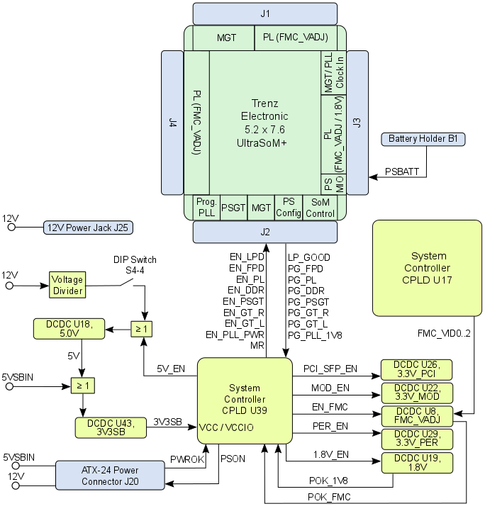
Figure 12: TEBF0808 Power-Management
Adjustable PL Bank VCCO Voltage FMC_VADJ
The carrier board VCCO voltage 'FMC_VADJ' supplying the PL IO-banks of the MPSoC (bank 64, 65, 66, 48) is provided by DC-DC converter U8 and selectable by the pins 'FMC_VID0' ... 'FMC_VID2' of the System Controller CPLD U17.
| FMC_VID2 | FMC_VID1 | FMC_VID0 | FMC_VADJ Value |
|---|---|---|---|
| 0 | 1 | 0 | 1.8V |
| 0 | 1 | 1 | 1.5V |
| 1 | 0 | 0 | 1.25V |
| 1 | 0 | 1 | 1.2V |
Table 3: Bit patterns for fixed values of the FMC_VADJ voltage
Note: These pins of the DC-DC converter U8 are hard-wired to initialiy fix the voltage to 1.8V (see schematic).
Power Distribution Dependencies
All on-board voltages of the TEBF0808 are generated out of the extern applied 12V power supply.
There are following dependencies how the initial 12V power supply is distributed to the on-board DC-DC converters, which power up further DCDC converters and the particular on-board voltages:
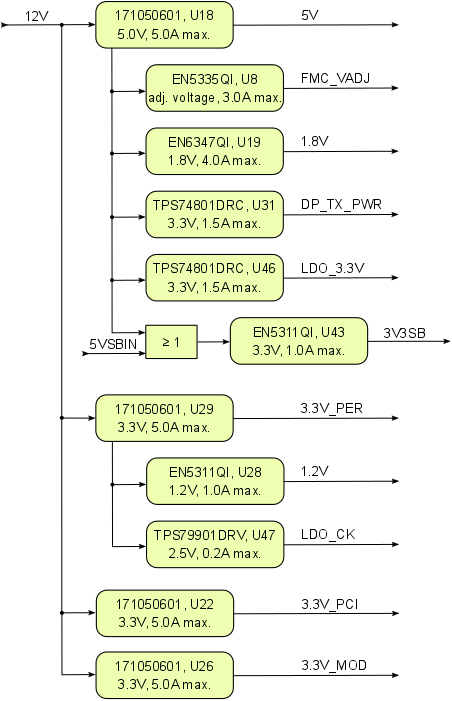
Figure 13: Power Distribution Diagram
Current rating of Samtec Razor Beam™ LSHM B2B connectors is 2.0A per pin (2 adjacent pins powered).
Power-On Sequence Diagram
The power-on sequence of the on-board DC-DC converters depens on the current firmware of the System Controller CPLD U17.
Following diagram visualizes the connection of the DC-DC converter control signals ('Enable', 'Power-Good') with System Controller CPLD U17, which enables the particular on-board voltages.
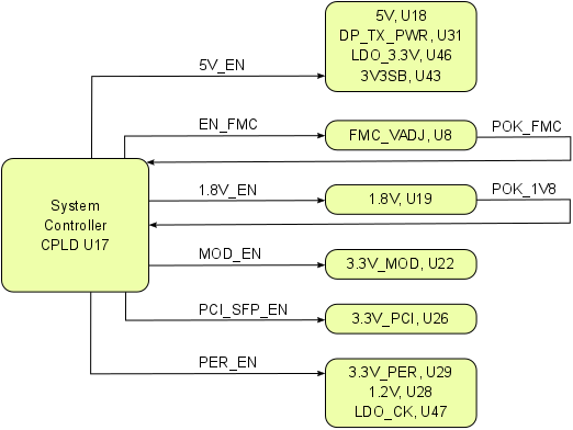
Figure 14: Power-On Sequence Utilizing DCDC Converter Control Signals
To avoid any damages to the MPSoC module, check for stabilized on-board voltages in steady state before powering up the MPSoC's I/O bank voltages VCCOx. All I/O's should be tri-stated during power-on sequence.
Core voltages and main supply voltages of the Zynq Ultrascale+ MPSoC have to reach stable state and the "Power Good"-signals of the SoM have to be asserted before other voltages like bank's I/O voltages (VCCOx) can be powered up.
It is important that all PS and PL I/Os are tri-stated at power-on until the "Power Good"-signals are logically high, meaning that all on-module voltages have become stable and module is properly powered up.
B2B connectors
Unable to render {include} The included page could not be found.
Technical Specifications
Absolute Maximum Ratings
Parameter | Min | Max | Unit | Notes / Reference Document |
|---|---|---|---|---|
| Power supply voltage (12V nominal) | 11.4 | 12.6 | V | ANSI/VITA 57.1 FPGA Mezzanine Card (FMC) standard |
| Battery Voltage PSBATT | -0.5 | 2 | V | Xilinx DS925 data sheet |
| Voltage on pins of PMOD P2 | -0.5 | 3.75 | V | MachXO2 Family Data Sheet |
Storage temperature (ambient) | -55 | 85 | °C | Marvell 88E1512 datasheet |
Assembly variants for higher storage temperature range are available on request.
Recommended Operating Conditions
| Parameter | Min | Max | Unit | Notes / Reference Document |
|---|---|---|---|---|
| Power supply voltage (12V nominal) | 11.4 | 12.6 | V | ANSI/VITA 57.1 FPGA Mezzanine Card (FMC) standard |
| Battery Voltage PSBATT | 1.2 | 1.5 | V | Xilinx DS925 data sheet |
| Voltage on pins PMOD P1 | 3.135 | 3.6 | V | MachXO2 Family Data Sheet |
Please check TRM TE0808 and Xilinx datasheet DS925 for complete list of absolute maximum and recommended operating ratings for the mounted TE0808 SoM.
Operating Temperature Ranges
Commercial grade: 0°C to +70°C.
Industrial grade: -40°C to +85°C.
Extended grade: 0°C to +85°C.
The module operating temperature range depends also on customer design and cooling solution. Please contact us for options.
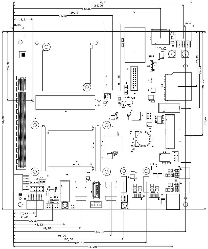
Physical Dimensions
Module size: 170 mm × 170 mm. Please download the assembly diagram for exact numbers
Mating height with standard connectors: 5 mm
PCB thickness: 1.844 mm ± 10%
Highest part on PCB: approx. 32 mm. Please download the step model for exact numbers
All dimensions are given in millimeters.
Revision History
Hardware Revision History
| Date | Revision | Notes | Link to PCN | Documentation Link |
|---|---|---|---|---|
| - | 04 | current available revision | - | TEBF0808-04 |
| - | 03 | Second production release | - | TEBF0808-03 |
| - | 02 | First production release | - | TEBF0808-02 |
| - | 01 | Prototype | - | - |
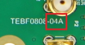
Hardware revision number is written on the PCB board together with the module model number separated by the dash.
Document Change History
| Date | Revision | Contributors | Description |
|---|---|---|---|
| Ali Naseri | Initial document |
Disclaimer
Data Privacy
Please also note our data protection declaration at https://www.trenz-electronic.de/en/Data-protection-Privacy
Document Warranty
The material contained in this document is provided “as is” and is subject to being changed at any time without notice. Trenz Electronic does not warrant the accuracy and completeness of the materials in this document. Further, to the maximum extent permitted by applicable law, Trenz Electronic disclaims all warranties, either express or implied, with regard to this document and any information contained herein, including but not limited to the implied warranties of merchantability, fitness for a particular purpose or non infringement of intellectual property. Trenz Electronic shall not be liable for errors or for incidental or consequential damages in connection with the furnishing, use, or performance of this document or of any information contained herein.
Limitation of Liability
In no event will Trenz Electronic, its suppliers, or other third parties mentioned in this document be liable for any damages whatsoever (including, without limitation, those resulting from lost profits, lost data or business interruption) arising out of the use, inability to use, or the results of use of this document, any documents linked to this document, or the materials or information contained at any or all such documents. If your use of the materials or information from this document results in the need for servicing, repair or correction of equipment or data, you assume all costs thereof.
Copyright Notice
No part of this manual may be reproduced in any form or by any means (including electronic storage and retrieval or translation into a foreign language) without prior agreement and written consent from Trenz Electronic.
Technology Licenses
The hardware / firmware / software described in this document are furnished under a license and may be used /modified / copied only in accordance with the terms of such license.
Environmental Protection
To confront directly with the responsibility toward the environment, the global community and eventually also oneself. Such a resolution should be integral part not only of everybody's life. Also enterprises shall be conscious of their social responsibility and contribute to the preservation of our common living space. That is why Trenz Electronic invests in the protection of our Environment.
REACH, RoHS and WEEE
REACH
Trenz Electronic is a manufacturer and a distributor of electronic products. It is therefore a so called downstream user in the sense of REACH. The products we supply to you are solely non-chemical products (goods). Moreover and under normal and reasonably foreseeable circumstances of application, the goods supplied to you shall not release any substance. For that, Trenz Electronic is obliged to neither register nor to provide safety data sheet. According to present knowledge and to best of our knowledge, no SVHC (Substances of Very High Concern) on the Candidate List are contained in our products. Furthermore, we will immediately and unsolicited inform our customers in compliance with REACH - Article 33 if any substance present in our goods (above a concentration of 0,1 % weight by weight) will be classified as SVHC by the European Chemicals Agency (ECHA).
RoHS
Trenz Electronic GmbH herewith declares that all its products are developed, manufactured and distributed RoHS compliant.
WEEE
Information for users within the European Union in accordance with Directive 2002/96/EC of the European Parliament and of the Council of 27 January 2003 on waste electrical and electronic equipment (WEEE).
Users of electrical and electronic equipment in private households are required not to dispose of waste electrical and electronic equipment as unsorted municipal waste and to collect such waste electrical and electronic equipment separately. By the 13 August 2005, Member States shall have ensured that systems are set up allowing final holders and distributors to return waste electrical and electronic equipment at least free of charge. Member States shall ensure the availability and accessibility of the necessary collection facilities. Separate collection is the precondition to ensure specific treatment and recycling of waste electrical and electronic equipment and is necessary to achieve the chosen level of protection of human health and the environment in the European Union. Consumers have to actively contribute to the success of such collection and the return of waste electrical and electronic equipment. Presence of hazardous substances in electrical and electronic equipment results in potential effects on the environment and human health. The symbol consisting of the crossed-out wheeled bin indicates separate collection for waste electrical and electronic equipment.
Trenz Electronic is registered under WEEE-Reg.-Nr. DE97922676.
Overview
Content Tools