Download PDF version of this document.
Table of Contents
Overview
The Trenz Electronic TEF1001 FPGA board is a PCI Express form factor card integrating the Xilinx Kintex-7 XC7K160T, XC7K325T or XC7K410T FPGA SoC. The FPGA-board is designed for high system resources and intended for use in applications with high demands on system performance and throughput. To extent the board with standard DDR3 SDRAM memory module, there is a 204-pin SODIMM socket with 64bit databus width on the board present. Highspeed data transmission is enabled by the 4 lane PCIe Gen 2 interface.
The board offers a HPC (High Pin Count) ANSI/VITA 57.1 compatible FMC interface connector for standard FPGA Mezzanine cards and modules. Other interface connectors found on-board include JTAG for accessing FPGA and on-board System Controller CPLD.
The TEF1001 FPGA board is intended to be used as add-on card in a PCIe 2.0 or higher capable host system to meet the power supply requirements.
Key Features
- Xilinx Kintex-7 XC7K160T, XC7K325T or XC7K410T FPGA SoC
- Large number of configurable I/Os are provided via HPC FMC connector
- 4 GTX high-performance transceiver
- 2x MGT transceiver clock inputs
- 160 FPGA I/O's (80 LVDS pairs)
- On-board high-efficiency switch-mode DC-DC converters
- Lattice MachXO2 LCMXO2-1200HC System Controller CPLD
- 10x User LEDs
- PCI Express x8 connector with 4 lane PCIe Gen 2 interface
- ANSI Vita 57.1 FMC High Pin Count (HPC) connector
- DDR3 SODIMM SDRAM socket with 64bit databus width
- 256Mbit (32MByte) Quad SPI Flash memory (for configuration and operation) accessible through:
- FPGA
- JTAG port (SPI indirect, bus width x4)
- FPGA configuration through:
- JTAG connector
- Quad SPI Flash memory
Clocking
Si5338 programmable quad PLL clock generator - 4 outputs for MGT and PL clocks
200MHz oscillator for DDR3 bank
- System management and power sequencing
Additional assembly options are available for cost or performance optimization upon request.
Block Diagram
TEF1001-02 block diagram
Main Components
TEF1001-02 main components
- Xilinx Kintex XC7K-2FBG676I FPGA SoC, U6
- ANSI/VITA 57.1 compliant FMC HPC connector, J2
- Cooling fan 5VDC M1 (45X5MM, 0.7W, 1.06CFM), M1
- PCIe x8 connector, J1
- DDR3 SODIMM 204-pin socket, U2
- 6-pin 12V power connector, J5
- Step-down DC-DC converter @1.5V and @4V (LT LTM4676A), U3
- Step-down DC-DC converter @1.0V (LT LTM4676A), U4
- 256 Mbit Quad SPI Flash Memory (Micron N25Q256A), U12
- 10x Green user LEDs connected to FPGA, D1 ... D10
- 4-wire PWM fan connector, J4
- User button, S2
- FPGA JTAG connector, J9
- 4bit DIP switch, S1
- I²C header for LTM4676A DC-DC converter, J10
- System Controller CPLD JTAG header, J8
- 1x Green LED connected to SC CPLD, D11
- 2-pin 5V FAN header, J6
- System Controller CPLD (Lattice Semiconductor LCMXO2-1200HC), U5
- 6A PowerSoC DC-DC converter @FMC_VADJ (Altera EN5365QI), U7
- 4A PowerSoC DC-DC converter @3.3V (3V3FMC) (Altera EN6347QI), U15
- LDO converter @1.2V (MGTAVTT_FPGA) (TI TPS74401RGW), U17
- LDO converter @1.0V (MGTAVCC_FPGA) (TI TPS74401RGW), U18
- 4A PowerSoC DC-DC converter @1.8V (Altera EN6347QI), U7
Initial Delivery State
| Storage device name | Content | Notes |
|---|---|---|
| Si5338A OTP Area | not programmed | - |
SPI Flash OTP Area | Empty, not programmed | Except serial number programmed by flash vendor |
SPI Flash Quad Enable bit | Programmed | - |
SPI Flash main array | demo design | - |
| HyperFlash Memory | not programmed | - |
eFUSE USER | Not programmed | - |
eFUSE Security | Not programmed | - |
Initial delivery state of programmable devices on the module
Control Signals
To get started with TEF1001 board, some basic control signals are essential and are described in the following table:
Control signal | Switch / Button / LED / Pin | Signal Schematic Names | Connected to | Functionality | Notes |
|---|---|---|---|---|---|
| SC CPLD JTAG Enable | DIP switch S3-3 | JTAGEN | SC CPLD U14, pin 82 | ON: SC CPLD JTAG enabled, | - |
| BOOT MODE | SC CPLD U14, pin 27 | MODE | B2B JB1, pin 31 | Boot Mode for attached module (Flash or SD) | - |
| Module Reset | SC CPLD U14, pin 13 | RESIN | B2B JB2, pin 17 | Module Reset | - |
| Global Reset input | Push Button S2 | S2 | SC CPLD U14, pin 2 | Manual reset from user | - |
| SD Card detection | SD Slot J8, pin 10 | SD_DETECT | SC CPLD U14, pin 40 | Detection Signal for inserted SD Card | Boot mode is set to SD Boot, when SD Card is detected. |
| Board status indicators | Red LEDs D1 ... D8 | ULED1 ... ULED8 | SC CPLD U14, pins 78, 77, 76, 16, 69, 68, 65, 64 | indicating various board and module status / configuration | Refer to the firmware documentation of the SC CPLD U14 and to the subsection 'LEDs' in section 'On-board Peripherals' for more details and current functionality. |
| Board 3.3V power indicator | Green LED D22 | 3V3IN | B2B JB1, pin 14, 16 | ON: 3.3V on-board voltage available | - |
| FMC_VADJ voltage selection | DIP switches S4-1, S4-2, S4-3 | VID0 ... VID2 | SC CPLD U14, pins 34, 35, 38 | sets adjustable voltage for FMC connector | - |
| I²C control / FMC_VADJ voltage selection | DIP switches S3-2, S3-1 | CM0, CM1 | SC CPLD U14, pins 99, 1 | enabling / disabling I²C control of board functionalities, sets FMC_VADJ voltage (only 3 steps), available to user if FMC_VADJ set by DIP-switch S4 | Refer to the firmware documentation of the SC CPLD U14 and and to the subsection 'DIP switches' in section 'On-board Peripherals' for current functionality and more details. |
TE0701 Control Signals
By default the configuration mode pins M[2:0] of the FPGA are set to QSPI mode (Master SPI), hence the FPGA is configured from QSPI Flash memory at system start-up. The JTAG interface of the module is provided for storing the initial FPGA configuration data to the QSPI Flash memory.
Signals, Interfaces and Pins
FMC HPC Connector
I/O signals and interfaces connected to the FPGA SoCs I/O bank and FMC connector J2:
| Interfaces | I/O Signal Count | LVDS-pairs count | Connected to | VCCO bank Voltage | Notes |
|---|---|---|---|---|---|
| I/O | 48 | 24 | FPGA Bank 12 HR | FMC_VADJ | Bank voltage FMC_VADJ is supplied by DC-DC converter U7 |
| 34 | 17 | FPGA Bank 13 HR | FMC_VADJ | ||
| 34 | 17 | FPGA Bank 15 HR | FMC_VADJ | ||
| 44 | 44 | FPGA Bank 16 HR | VIO_B_FMC | Bank voltage VIO_B_FMC is supplied by FMC connector J2 | |
| I²C | 2 | - | SC CPLD U5, Bank 2, pin 48, 49 | - | FMC connector J2 is hardware programmed to I²C address 0x50 |
| JTAG | 5 | - | SC CPLD U5, Bank 2, pin 27, 28, 331, 32 ,36 | 3.3V | 4 JTAG pins with additional signal 'TRST' |
| MGT | - | 8 (4 x RX/TX) | Bank 116 GTX | - | 4x MGT lanes |
| Clock Input | - | 2 | Bank 116 GTX | - | 2x Reference clock input to MGT bank |
| Control Signals | 3 | - | SC CPLD U5, Bank 1, pin 68, 69 ,70 | 3.3V | 'FMC_PG_C2M', 'FMC_PG_M2C', 'FMC_PRSNT_M2C_L' |
Table 2: FMC connector J2 interface
For detailed information about the pin out, please refer to the Pin-out Tables.
FMC connector J2 MGT Lanes:
| MGT Lane | Bank | Type | Signal Schematic Name | FMC Connector Pin | FPGA Pin |
|---|---|---|---|---|---|
| 0 | 116 | GTX |
|
|
|
| 1 | 116 | GTX |
|
|
|
| 2 | 116 | GTX |
|
|
|
| 3 | 116 | GTX |
|
|
|
Table 3: FMC connector J2 MGT lanes
FMC connector J2 reference clock sources:
| Signal Schematic Name | Connected to | FMC Connector Pin | FPGA Pin | Notes |
|---|---|---|---|---|
| MGT bank 116 | J2-D4 | MGTREFCLK0P_116, D6 | Supplied by attached FMC module |
| MGT bank 116 | J2-B20 J2-B21 | MGTREFCLK1P_116, F6 MGTREFCLK1N_116, F5 | Supplied by attached FMC module |
Table 4: FMC connector J2 clock signal input
FMC connector J2 VCC/VCCIO:
| Available VCC/VCCIO | FMC Connector Pin | Source | Notes |
|---|---|---|---|
| 3V3FMC | J2-D36 | DCDC U15, | Enable by SC CPLD U5, bank 1, pin 60 |
| 3V3 | J2-D32 | LDO U9, max. current: 0.5A | not dedicated for FMC connector |
| 12V | J2-C35 | external source through | - |
| FMC_VADJ | J2-H40 | DCDC U7, | Enable by SC CPLD U5, bank 1, pin 51 |
Table 5: FMC connector J2 available VCC/VCCIO
FMC connector J2 Cooling Fan:
| Fan Designator | Enable Signal | Notes |
|---|---|---|
| M1 | Enable by SC CPLD U5, bank 0, pin 78 | - |
Table 6: FMC connector J2 cooling fan
PCI Express Interface
The TEF1001 FPGA board is a PCI Express card designed to fit into systems with PCI Express x8 slots and has a data transmission capability which meets PCIe Gen. 2 with 4 GTX lanes routed to the PCIe interface.
Following table lists lane number, MGT bank number, transceiver type, signal schematic name, connector and FPGA pins connection:
| Lane | Bank | Type | Signal Name | PCIe Connector Pin | FPGA Pin |
|---|---|---|---|---|---|
| 0 | 115 | GTX |
|
|
|
| 1 | 115 | GTX |
|
|
|
| 2 | 115 | GTX |
|
|
|
| 3 | 115 | GTX |
|
|
|
Table 7: GTX lanes routed to the PCIe interface
| PCIe | Signal Schematic Name | Connected to | PCIe connector pin | FPGA Pin | Notes |
|---|---|---|---|---|---|
J1 |
| MGT bank 115 | J1-A13, REFCLK+ | MGTREFCLK1P_115, K6 | External clock supplied by PCIe interface |
Table 8: PCIe reference clock sources
JTAG Connectors
There are two JTAG connectors J8 and J9 available on the TEF1001 board:
| JTAG Interface | Signal Schematic Name | JTAG Connector Pin | Connected to |
|---|---|---|---|
CPLD JTAG VCCIO: 3.3V Connector: J8 | CPLD_JTAG_TMS | J8-1 | SC CPLD, bank 0, pin 90 |
| CPLD_JTAG_TDI | J8-2 | SC CPLD, bank 0, pin 94 | |
| CPLD_JTAG_TDO | J8-3 | SC CPLD, bank 0, pin 95 | |
| CPLD_JTAG_TCK | J8-4 | SC CPLD, bank 0, pin 91 | |
FPGA JTAG VCCIO: 1.8V Connector: J9 | FPGA_JTAG_TMS | J9-4 | FPGA, bank 0, pin N9 |
| FPGA_JTAG_TCK | J9-6 | FPGA, bank 0, pin M8 | |
| FPGA_JTAG_TDO | J9-8 | FPGA, bank 0, pin N8 | |
| FPGA_JTAG_TDI | J9-10 | FPGA, bank 0, pin L8 |
Table 9: JTAG interface signals
FAN Connectors
The TEF1001 board offers one FAN connector for cooling the FPGA device and one built-in FAN for the FMC modules.
| Connector | Signal Schematic Names | Connected to | Notes |
|---|---|---|---|
| 4-Wire PWM FAN connector J4, 12V power supply | 'F1SENSE', pin J4-3 | SC CPLD U5, pin 99 | FPGA cooling FAN can be controlled via I²C interface from FPGA, see current SC CPLD firmware |
| 2-pin FAN connector J6, 5V power supply with TPS2051 Load Switch U25 | 'FAN_FMC_EN', (Load Switch U25, pin 4) | SC CPLD U5, pin 78 | FMC cooling FAN |
Table 10: FAN connectors
On-board Peripherals
System Controller CPLD
The System Controller CPLD (U5) is provided by Lattice Semiconductor LCMXO2-256HC (MachXO2 Product Family). The SC-CPLD is the central system management unit where essential control signals are logically linked by the implemented logic in CPLD firmware, which generates output signals to control the system, the on-board peripherals and the interfaces. Interfaces like JTAG and I2C between the on-board peripherals and to the FPGA module are by-passed, forwarded and controlled by the System Controller CPLD.
Other tasks of the System Controller CPLD are the monitoring of the power-on sequence and to display the programming state of the FPGA module.
For detailed information, refer to the reference page of the SC CPLD firmware of this module. Table below lists the SC CPLD I/O pins with their default configuration:
| SC CPLD U5 Pins and Interfaces | Connected to | Function | Notes |
|---|---|---|---|
| 200MHZCLK_EN | Oscillator U1, pin 1 | Oscillator U1 control line | enables 200.0000MHz oscillator U1 |
| BUTTON | Push Button S2 | user | Reset Button |
| CPLD_JTAG_TDO | header J8, pin 3 | SC CPLD JTAG interface | SC CPLD JTAG interface enabled when DIP-switch S1-1 in ON-position |
| CPLD_JTAG_TDI | header J8, pin 2 | ||
| CPLD_JTAG_TCK | header J8, pin 4 | ||
| CPLD_JTAG_TMS | header J8, pin 1 | ||
| JTAG_EN | DIP switch S1-1 | ||
| DDR3_SCL | SO-DIMM U2. pin 202 | I²C bus of DDR3 SO-DIMM | I²C interface connected to FPGA |
| DDR3_SDA | SO-DIMM U2. pin 200 | ||
| PLL_SCL | Si5338 U13, pin 12 | I²C bus of SI5338 quad clock PLL | I²C interface connected to FPGA |
| PLL_SDA | Si5338 U13, pin 19 | ||
| PCIE_RSTb | PCIe J1, pin A11 | PCIe reset input | refer to current SC CPLD firmware for functionality |
| FEX_DIR / FEX0 ... FEX11 | FPGA bank 14 | user GPIO | refer to current SC CPLD firmware for functionality |
| F1PWM | FAN connector J4, pin 4 | FPGA FAN control | refer to current SC CPLD firmware for functionality |
| F1SENSE | FAN connector J4, pin 3 | ||
| FAN_FMC_EN | Load Switch U25, pin 4 | FMC FAN enable | |
| FMC_PG_C2M | FMC J2, pin D1 | FMC control signals | refer to current SC CPLD firmware for functionality |
| FMC_PG_M2C | FMC J2, pin F1 | ||
| FMC_PRSNT_M2C_L | FMC J2, pin H2 | ||
| FMC_SCL | FMC J2, pin C30 | FMC I²C | I²C connected to FPGA |
| FMC_SDA | FMC J2, pin C31 | ||
| FMC_TCK | FMC J2, pin D29 | FMC JTAG | refer to current SC CPLD firmware for functionality |
| FMC_TDI | FMC J2, pin D30 | ||
| FMC_TDO | FMC J2, pin D31 | ||
| FMC_TMS | FMC J2, pin D33 | ||
| FMC_TRST | FMC J2, pin D34 | ||
| DONE | FPGA bank 0, pin J7 | FPGA configuration signal | PL configuration completed |
| PROGRAM_B | FPGA bank 0, pin P6 | PL configuration reset signal | |
| LED1 | Green LED D11 | LED status signal | refer to current SC CPLD firmware for functionality |
| FPGA_IIC_OE | FPGA bank 14, pin F25 | SC CPLD works as I²C switch with the FPGA as I²C-Master and on-board peripherals as I²C-Slaves | I²C output enable |
| FPGA_IIC_SCL | FPGA bank 14, pin G26 | I²C clock line | |
| FPGA_IIC_SDA | FPGA bank 14, pin G25 | I²C data line | |
| EN_1V8 | DC-DC U20, pin 27 | Power control | enable signal DC-DC U20 |
| PG_1V8 | DC-DC U20, pin 28 | power good signal DC-DC U20 | |
| EN_3V3FMC | DC-DC U15, pin 27 | enable signal DC-DC U15 | |
| PG_3V3 | DC-DC U15, pin 28 | power good signal DC-DC U15 | |
| EN_FMC_VADJ | DC-DC U7, pin 52 | enable signal DC-DC U7 | |
| PG_FMC_VADJ | DC-DC U7, pin 46 | power good DC-DC U7 | |
VID0_FMC_VADJ, | DC-DC U7, pin 45, 44, 43 | DCDC U7 power selection pin | |
VID0_FMC_VADJ_CTRL, | DIP switch S1-2, DIP switch S1-3, DIP switch S1-4 | Power selection of FMC_VADJ, forwarded to DCDC U7 | |
| LTM_1V5_RUN | DC-DC U3, pin F5 | enable signals of DCDC U3, U4 (LTM4676) refer to current SC CPLD firmware for functionality | |
| LTM_4V_RUN | DC-DC U3, pin F5 | ||
| LTM_SCL | DC-DC U3 / U4, pin E6 | DCDC U3, U4 (LTM4676) I²C | I²C Address U3: 0x40 I²C Address U4: 0x4F I²C interface of LTM4676 ICs |
| LTM_SDA | DC-DC U3 / U4, pin D6 | ||
| LTM1_ALERT | DC-DC U4, pin E5 | DCDC U3, U4 (LTM4676) control, active low | refer to current SC CPLD firmware for functionality |
| LTM2_ALERT | DC-DC U3, pin E5 | ||
| LTM_1V_IO0 | DC-DC U4, pin E4 | ||
| LTM_1V_IO1 | DC-DC U4, pin F5 | ||
| LTM_1V5_4V_IO0 | DC-DC U3, pin E4 | ||
| LTM_1V5_4V_IO1 | DC-DC U3, pin F4 |
Table 11: System Controller CPLD I/O pins
For detailed function of the pins and signals, the internal signal assignment and the implemented logic, look to the Wiki reference page of the module's SC CPLD or into its bitstream file.
DDR3 SDRAM ECC SO-DIMM Socket
The TEF1001 board supports additional DDR3 ECC SO-DIMM via 204-pin socket U2. The DDR3 memory interface has a 64bit wide databus and is routed to the FPGA banks 32, 33 and 34.
The reference clock signal for the DDR3 interface is generated by the 200.0000MHz MEMS oscillator U1 and is applied to the FPGA bank 33.
There is also a I2C interface between the System Controller CPLD U5 and the DDR3 ECC SO-DIMM memory socket U2.
| I²C Interface | Schematic net names | Connected to | I²C Address | Notes |
|---|---|---|---|---|
| DDR3 SODIMM, U2 | 'DDR3_SDA', pin 200 | SC CPLD U5, pin 42 | module dependent | - |
Table 12: DDR3 SODIMM socket I²C interface
It is important to use SO-DIMMs which also provide ECC functionality. Otherwise the SO-DIMM is not compatible with this board.
Quad SPI Flash Memory
A 256 Mbit (32 MByte) Quad SPI Flash Memory (Micron N25Q256A, U12) is provided for FPGA configuration file storage. After configuration process completes the remaining free memory can be used for application data storage. All four SPI data lines are connected to the FPGA allowing x1, x2 or x4 data bus widths to be used. The maximum data transfer rate depends on the bus width and clock frequency. The memory can be accessed indirectly by the FPGA JTAG port (J9) by implementing the functional logic for this purpose inside the FPGA.
Quad SPI Flash memory interface is connected to the FPGA bank 14, QSPI clock is provided by FPGA config bank 0.
| Signal Name | QSPI Flash Memory U12 Pin | FPGA Pin |
|---|---|---|
| FLASH_QSPI_CS | S, Pin 7 | Bank 14, Pin C23 |
| FLASH_QSPI_D00 | DQ0, Pin 15 | Bank 14, Pin B24 |
| FLASH_QSPI_D01 | DQ1, Pin 8 | Bank 14, Pin A25 |
| FLASH_QSPI_D02 | DQ2, Pin 9 | Bank 14, Pin B22 |
| FLASH_QSPI_D03 | DQ3, Pin 1 | Bank 14, Pin A22 |
| FPGA_CFG_CCLK | C, Pin 16 | Bank 0, Pin C8 |
Table 13: Quad SPI interface signals and connections
SPI Flash QE (Quad Enable) bit must be set to high or FPGA is unable to load its configuration from flash during power-on. By default this bit is set to high at the manufacturing plant.
Programmable Clock Generator
There is a Silicon Labs I2C programmable quad PLL clock generator on-board (Si5338A, U13) to generate various reference clocks for the module.
| Si5338A Pin | Signal Name / Description | Connected to | Direction | Note |
|---|---|---|---|---|
IN1 | - | not connected | Input | not used |
| IN2 | - | GND | Input | not used |
IN3 | Reference input clock | U3, pin 3 | Input | 25.000000 MHz oscillator U14, Si8208AI |
IN4 | - | GND | Input | I2C slave device address LSB |
IN5 | - | not connected | Input | not used |
| IN6 | - | GND | Input | not used |
| SCL | PLL_SCL | SC CPLD U5, pin 8 | Input / Output | I²C interface muxed to FPGA Slave address: 0x70. |
| SDA | PLL_SDA | SC CPLD U5, pin 2 | Input / Output | |
CLK0A | CLK0_P | U6, G24 | Output | Clock to PL bank 14 |
| CLK0B | CLK0_N | U6, F24 | ||
| CLK1A | MGTCLK_5338_P | U6, H6 | Output | Clock to MGT bank 115, |
| CLK1B | MGTCLK_5338_N | U6, H5 | ||
| CLK2A | CLK1_P | U6, G22 | Output | Clock to PL bank 14 |
| CLK2B | CLK1_N | U6, F23 | ||
| CLK3A | CLK2_P | U6, D23 | Output | Clock to PL bank 14 |
| CLK3B | CLK2_N | U6, D24 |
Table 14: Programmable quad PLL clock generator inputs and outputs
Oscillators
The FPGA module has following reference clocking sources provided by on-board oscillators and FMC connector J2:
| Clock Source | Frequency | Signal Schematic Name | Clock Destination | Notes |
|---|---|---|---|---|
| U14, SiT8208AI | 25.000000 MHz | CLK | Si5338A PLL U13, pin 3 (IN3) | - |
| U1, DSC1123DL5 | 200.0000 MHz | DDR3_CLK_P | FPGA bank 33, pin AB11 | Enable by SC CPLD U5, pin 30 Signal: '200MHzCLK_EN' |
| DDR3_CLK_N | FPGA bank 33, pin AC11 | |||
| FMC Connector J2 | - | GBTCLK0_M2C_P, Pin J2-D4 | FPGA bank 116, pin D6 | reference clock to MGT bank 116 |
| GBTCLK0_M2C_N, Pin J2-D5 | FPGA bank 116, pin D5 | |||
| - | GBTCLK1_M2C_P, Pin J2-B20 | FPGA bank 116, pin F6 | reference clock to MGT bank 116 | |
| GBTCLK1_M2C_N, Pin J2-B21 | FPGA bank 116, pin F5 | |||
| - | CLK0_M2C_P, Pin J2-H4 | FPGA bank 15, pin H17 | reference clock to PL bank 15 | |
| CLK0_M2C_N, Pin J2-H5 | FPGA bank 15, pin H18 | |||
| - | CLK1_M2C_P, Pin J2-G2 | FPGA bank 15, pin G17 | reference clock to PL bank 15 | |
| CLK1_M2C_N, Pin J2-G3 | FPGA bank 15, pin G18 | |||
| - | CLK2_BIDIR_P, Pin J2-K4 | FPGA bank 13, pin P23 | reference clock to PL bank 13 bidirectional clock line | |
| CLK2_BIDIR_N, Pin J2-K5 | FPGA bank 13, pin N23 | |||
| - | CLK3_BIDIR_P, Pin J2-J2 | FPGA bank 13, pin R22 | reference clock to PL bank 13 bidirectional clock line | |
| CLK3_BIDIR_N, Pin J2-J3 | FPGA bank 13, pin R23 |
Table 15: Reference clock signals
On-board LEDs
| LED | Color | Signal Schematic name | Connected to | Description and Notes |
|---|---|---|---|---|
| D1 | Green | FPGA_LED1_VT | FPGA bank 13, pin K25 | LEDs D1 to D10 are available to user. LED voltages are translated from FPGA bank 13 and 14 |
| D2 | Green | FPGA_LED2_VT | FPGA bank 13, pin K26 | |
| D3 | Green | FPGA_LED3_VT | FPGA bank 13, pin P26 | |
| D4 | Green | FPGA_LED4_VT | FPGA bank 13, pin R26 | |
| D5 | Green | FPGA_LED5_VT | FPGA bank 13, pin N16 | |
| D6 | Green | FPGA_LED6_VT | FPGA bank 14, pin J26 | |
| D7 | Green | FPGA_LED7_VT | FPGA bank 14, pin H26 | |
| D8 | Green | FPGA_LED8_VT | FPGA bank 14, pin E26 | |
| D9 | Green | FPGA_LED9_VT | FPGA bank 14, pin A24 | |
| D10 | Green | FPGA_LED10_VT | FPGA bank 15, pin F19 | |
| D11 | Green | LED1 | System Controller CPLD, bank 0, pin 76 | refer to current CPLD firmware for LED functionality |
Table 16: On-board LEDs
Configuration DIP-switch
There is one 4-bit DIP-witches S1 present on the TEB0911 board to configure options and set parameters. The following section describes the functionalities of the particular switches.
Table below describes the functionalities of the switches of DIP-switches S3 and S4 at their each positions:
| DIP-switch S3 | Signal Schematic Name | Connected to | Functionality | Notes |
|---|---|---|---|---|
| S1-1 | JTAG_EN | SC CPLD U5, bank 1, pin 82 | enables JTAG interface of SC CPLD U5 in ON-position | SC CPLD programmable through JTAG header J8 |
| S1-2 | VID0_FMC_VADJ_CTRL | SC CPLD U5, bank 1, pin 71 | set 3bit code to adjust FMC_VADJ voltage | The FMC_VADJ voltage is provided by DCDC U7 EN5365QI, the voltage can be adjusted from 0.8V to 3.3V in 7 steps: Set DIP-switches as bit pattern "S1-4 | S1-3 | S1-2: FMC_VADJ": 0 | 0 | 0 : 3.3V |
| S1-3 | VID1_FMC_VADJ_CTRL | SC CPLD U5, bank 1, pin 63 | ||
| S1-4 | VID2_FMC_VADJ_CTRL | SC CPLD U5, bank 1, pin 62 |
Table 17: DIP-switch S1 functionality description
Power and Power-On Sequence
Power Consumption
The maximum power consumption of a module mainly depends on the design running on the FPGA.
Xilinx provide a power estimator excel sheets to calculate power consumption. It's also possible to evaluate the power consumption of the developed design with Vivado. See also Trenz Electronic Wiki FAQ.
| Power Input | Typical Current |
|---|---|
| 12V VIN | TBD* |
Table 18: Typical power consumption
* TBD - To Be Determined soon with reference design setup.
It is recommended to connect the ATX connector J5 to a 12V power supply source with minimum current capability of 6A to provide a sufficient power source to the board. Only one power source is needed at the same time, the system disconnects automatically PCIe power supply from PCIe edge connector J1 if the board is powered by the ATX connector J5.
To avoid any damage to the module, check for stabilized on-board voltages should be carried out (i.e. power good and enable signals) before powering up any FPGA's I/O bank voltages VCCO_x. All I/Os should be tri-stated during power-on sequence.
Power Distribution Dependencies
Figure 3: TEF1001-02 Power Distribution Diagram
Power-On Sequence
The TEF1001 board meets the recommended criteria to power up the Xilinx FPGA properly by keeping a specific sequence of enabling the on-board DC-DC converters dedicated to the particular functional units of the FPGA chip and powering up the on-board voltages.
Some of the voltages are handled by the System Controller CPLD using "Power good"-signals from the voltage regulators:
Following diagram clarifies the sequence of enabling the particular on-board voltages, which will power-up in descending order as listed in the blocks of the diagram:
Figure 4: TEF1001-02 Power-On Sequence Diagram
Bank Voltages
| Bank | Schematic Name | Voltage | Range | Notes |
|---|---|---|---|---|
| 0 | 1V8 | 1.8V | - | Config bank 0 fixed to 1.8V |
| 12 | FMC_VADJ | user | HR: 1.2V to 3.3V | FMC_VADJ voltage ajustable by DIP switch S1 |
| 13 | FMC_VADJ | user | HR: 1.2V to 3.3V | FMC_VADJ voltage ajustable by DIP switch S1 |
| 14 | 1V8 | 1.8V | HR: 1.2V to 3.3V | PL bank 14 fixed to 1.8V |
| 15 | FMC_VADJ | user | HR: 1.2V to 3.3V | FMC_VADJ voltage ajustable by DIP switch S1 |
| 16 | VIO_B_FMC | user | HR: 1.2V to 3.3V | PL bank 16 fixed to 1.8V |
| 32 | 1V5 | 1.5V | HP: 1.2V to 1.8V | DDR3 memory interface |
| 33 | 1V5 | 1.5V | HP: 1.2V to 1.8V | DDR3 memory interface |
| 34 | 1V5 | 1.5V | HP: 1.2V to 1.8V | DDR3 memory interface |
115 116 | MGTAVCC_FPGA MGTVCCAUX_FPGA MGTAVTT_FPGA | 1.0V 1.8V 1.2V | MGT bank supply voltage MGT bank auxiliary supply voltage MGT bank termination circuits voltage | MGT banks with Xilinx GTX transceiver units |
Table 19: Board I/O bank voltages
Power Rails
| Connector / Pin | Voltage | Direction | Notes |
|---|---|---|---|
| J4, pin 2 | 12V | Output | 4-wire PWM fan connector supply voltage |
| J6, pin 2 | 5V | Output | Cooling fan M1 supply voltage |
| J8, pin 6 | 3V3 | Output | VCCIO CPLD JTAG |
| J9, pin 2 | 1V8 | Output | VCCIO FPGA JTAG |
| J2, pin C35 / C37 | 12V | Output | FMC supply voltage |
| J2, pin D32 | 3V3 | Output | VCCIO FMC |
| J2, pin D36 / D38 / D39 / D40 | 3V3FMC | Output | VCCIO FMC |
| J2, pin H1 | VREF_A_M2C | Input | VREF voltage for bank 13 / 15 |
| J2, pin K1 | VREF_B_M2C | Input | VREF voltage for bank 16 |
| J2, pin J39 / J40 | VIO_B_FMC | Input | PL I/O voltage bank 16 (VCCO) |
| J2, pin H40 / G39 / F40 / E39 | FMC_VADJ | Output | PL I/O voltage bank 12 / 13 / 15 (VCCO) |
| J1, pin B1 / B2 / B3 / A2 / A3 | 12V_input_B | Input | 12V main power supply from PCIe connector |
| J5, pin 1 / 2 / 3 | 12V_input_A | Input | Main power supply connector |
Table 20: Board power rails
Variants Currently In Production
See also the current available variants on the Trenz Electronic shop page
| Trenz shop TEF1001 overview page | |
|---|---|
| English page | German page |
Technical Specifications
Absolute Maximum Ratings
Parameter | Min | Max | Units | Reference Document |
|---|---|---|---|---|
VIN supply voltage | -0.3 | 20 | V | TPS6217 datasheet Note: voltage limitations are not valid for connected FMC module and/or FPGA FAN |
| Supply voltage for HR I/O banks (VCCO) | -0.500 | 3.600 | V | Xilinx datasheet DS182 |
Supply voltage for HP I/O banks (VCCO) | -0.500 | 2.000 | V | Xilinx datasheet DS182 |
| I/O input voltage for HR I/O banks | -0.500 | VCCO + 0.500 | V | Xilinx datasheet DS182 |
I/O input voltage for HP I/O banks | -0.500 | VCCO + 0.500 | V | Xilinx datasheet DS182 |
| Reference Voltage pin (VREF) | -0.500 | 2 | V | Xilinx datasheet DS182 |
| Differential input voltage | -0.5 | 2.625 | V | Xilinx datasheet DS182 |
| I/O input voltage for SC CPLD U5 | -0.5 | 3.75 | V | Lattice MachXO2 Family datasheet |
| GTX transceiver reference clocks absolute input voltage | -0.500 | 1.320 | V | Xilinx datasheet DS182 |
GTX transceiver receiver (RXP/RXN) and transmitter (TXP/TXN) absolute input voltage | -0.500 | 1.260 | V | Xilinx datasheet DS182 |
| Voltages on LTM4676 I²C pins (LTM_SCL, LTM_SDA), header J10 | -0.3 | 5.5 | V | LTM4676A datasheet |
Storage temperature | -40 | +100 | °C | SML-P11 LED datasheet |
Table 21: Module absolute maximum ratings
Assembly variants for higher storage temperature range are available on request.
Recommended Operating Conditions
| Parameter | Min | Max | Units | Reference Document |
|---|---|---|---|---|
| VIN supply voltage | 11.4 | 12.6 | V | 12V nominal, ANSI/VITA 57.1 power specification for FMC connector |
| Supply voltage for HR I/O banks (VCCO) | 1.140 | 3.465 | V | Xilinx datasheet DS182 |
Supply voltage for HP I/O banks (VCCO) | 1.140 | 1.890 | V | Xilinx datasheet DS182 |
I/O input voltage for HR I/O banks | -0.500 | VCCO + 0.20 | V | Xilinx datasheet DS182 |
| I/O input voltage for HP I/O banks | -0.500 | VCCO + 0.20 | V | Xilinx datasheet DS182 |
| Differential input voltage | -0.2 | 2.625 | V | Xilinx datasheet DS182 |
| I/O input voltage for SC CPLD U5 | -0.3 | 3.6 | V | Lattice MachXO2 Family datasheet |
| Voltages on LTM4676 I²C pins (LTM_SCL, LTM_SDA), header J10 | 0 | 3.3V | V | LTM4676A datasheet |
Board Operating Temperature Range 1), 2) | -40 | 85 | °C | board operating temperature range limited by FPGA SoC and on-board peripherals |
Table 22: Module recommended operating conditions
1) Temperature range may vary depending on assembly options
2) The operating temperature range of the FPGA soC and on-board peripherals are junction and also ambient operating temperature ranges
Board operating temperature range depends also on customer design and cooling solution. Please contact us for options.
Please check also Xilinx datasheet DS182 for complete list of absolute maximum and recommended operating ratings.
Physical Dimensions
Board size: 167.65mm × 106.65mm. Please download the assembly diagram for exact numbers.
PCB thickness: ca. 1.55mm.
The board meets the PCIe Card Electromechanical specifications Revision 1.1
All dimensions are given in millimeters.
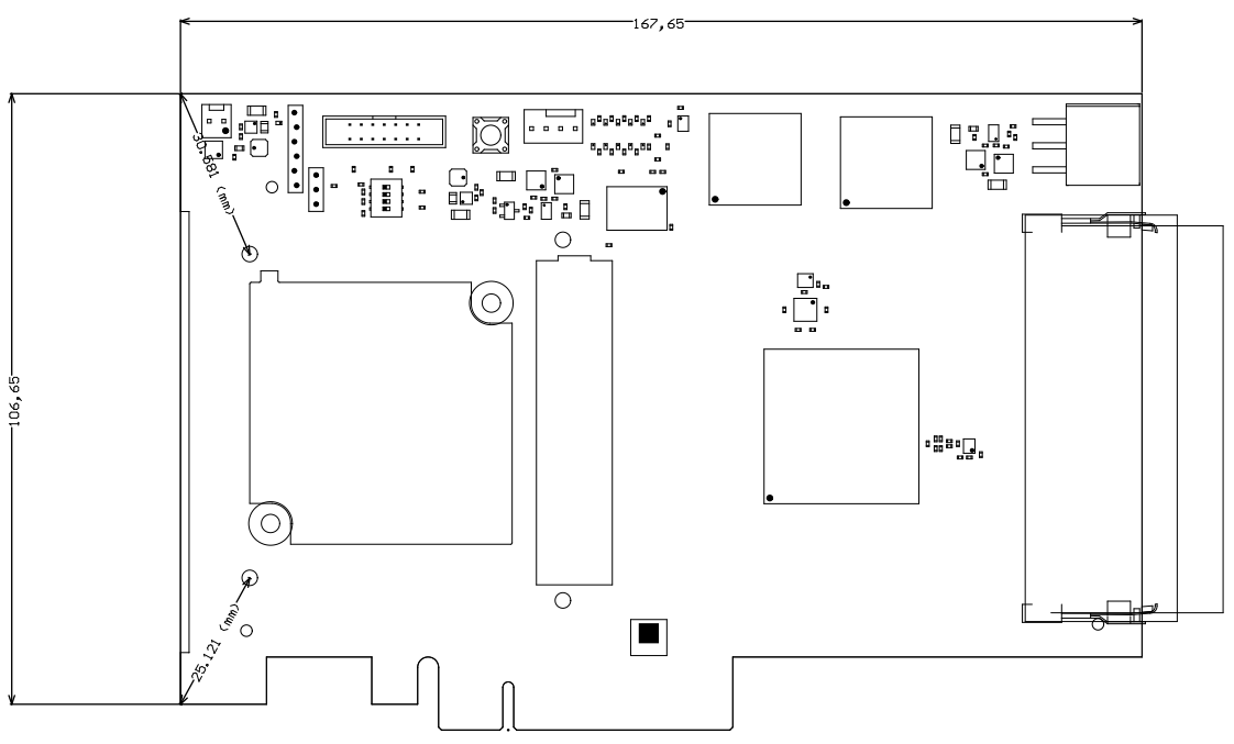
Figure 5: Module physical dimensions drawing
Revision History
Hardware Revision History
| Date | Revision | Notes | PCN | Documentation Link |
|---|---|---|---|---|
| - | 02 | current available board revision | - | - |
| - | 01 | First production release | PCN-20180524 TEF1001-01 | TEF1001-01 |
Table 23: Module hardware revision history
Hardware revision number can be found on the PCB board together with the module model number separated by the dash.
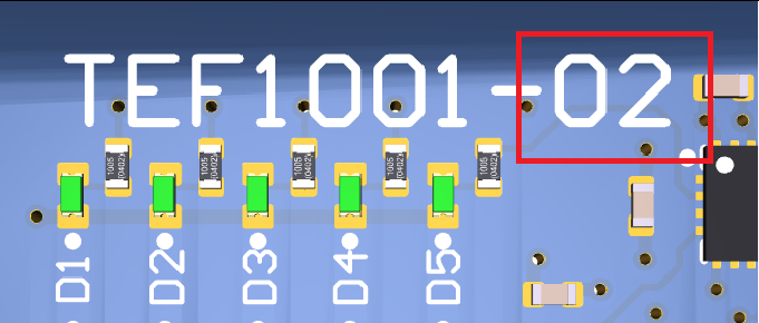
Figure 6: Module hardware revision number
Document Change History
Date | Revision | Contributors | Description |
|---|---|---|---|
|
Table 24: Document change history
Disclaimer
Data Privacy
Please also note our data protection declaration at https://www.trenz-electronic.de/en/Data-protection-Privacy
Document Warranty
The material contained in this document is provided “as is” and is subject to being changed at any time without notice. Trenz Electronic does not warrant the accuracy and completeness of the materials in this document. Further, to the maximum extent permitted by applicable law, Trenz Electronic disclaims all warranties, either express or implied, with regard to this document and any information contained herein, including but not limited to the implied warranties of merchantability, fitness for a particular purpose or non infringement of intellectual property. Trenz Electronic shall not be liable for errors or for incidental or consequential damages in connection with the furnishing, use, or performance of this document or of any information contained herein.
Limitation of Liability
In no event will Trenz Electronic, its suppliers, or other third parties mentioned in this document be liable for any damages whatsoever (including, without limitation, those resulting from lost profits, lost data or business interruption) arising out of the use, inability to use, or the results of use of this document, any documents linked to this document, or the materials or information contained at any or all such documents. If your use of the materials or information from this document results in the need for servicing, repair or correction of equipment or data, you assume all costs thereof.
Copyright Notice
No part of this manual may be reproduced in any form or by any means (including electronic storage and retrieval or translation into a foreign language) without prior agreement and written consent from Trenz Electronic.
Technology Licenses
The hardware / firmware / software described in this document are furnished under a license and may be used /modified / copied only in accordance with the terms of such license.
Environmental Protection
To confront directly with the responsibility toward the environment, the global community and eventually also oneself. Such a resolution should be integral part not only of everybody's life. Also enterprises shall be conscious of their social responsibility and contribute to the preservation of our common living space. That is why Trenz Electronic invests in the protection of our Environment.
REACH, RoHS and WEEE
REACH
Trenz Electronic is a manufacturer and a distributor of electronic products. It is therefore a so called downstream user in the sense of REACH. The products we supply to you are solely non-chemical products (goods). Moreover and under normal and reasonably foreseeable circumstances of application, the goods supplied to you shall not release any substance. For that, Trenz Electronic is obliged to neither register nor to provide safety data sheet. According to present knowledge and to best of our knowledge, no SVHC (Substances of Very High Concern) on the Candidate List are contained in our products. Furthermore, we will immediately and unsolicited inform our customers in compliance with REACH - Article 33 if any substance present in our goods (above a concentration of 0,1 % weight by weight) will be classified as SVHC by the European Chemicals Agency (ECHA).
RoHS
Trenz Electronic GmbH herewith declares that all its products are developed, manufactured and distributed RoHS compliant.
WEEE
Information for users within the European Union in accordance with Directive 2002/96/EC of the European Parliament and of the Council of 27 January 2003 on waste electrical and electronic equipment (WEEE).
Users of electrical and electronic equipment in private households are required not to dispose of waste electrical and electronic equipment as unsorted municipal waste and to collect such waste electrical and electronic equipment separately. By the 13 August 2005, Member States shall have ensured that systems are set up allowing final holders and distributors to return waste electrical and electronic equipment at least free of charge. Member States shall ensure the availability and accessibility of the necessary collection facilities. Separate collection is the precondition to ensure specific treatment and recycling of waste electrical and electronic equipment and is necessary to achieve the chosen level of protection of human health and the environment in the European Union. Consumers have to actively contribute to the success of such collection and the return of waste electrical and electronic equipment. Presence of hazardous substances in electrical and electronic equipment results in potential effects on the environment and human health. The symbol consisting of the crossed-out wheeled bin indicates separate collection for waste electrical and electronic equipment.
Trenz Electronic is registered under WEEE-Reg.-Nr. DE97922676.
Overview
Content Tools