Page History
...
| Page properties | ||||
|---|---|---|---|---|
| ||||
Template Revision 2.0 - on construction2 TRM Name always "TE Series Name" +TRM, for example, "TE0720 TRM" |
| HTML |
|---|
<style>
.wrapped{
  width: 100% !important;
  max-width: 1200px !important;
}
</style> |
...
| Page properties | |||||||||||||||||||||||||||||||||||||||||||
|---|---|---|---|---|---|---|---|---|---|---|---|---|---|---|---|---|---|---|---|---|---|---|---|---|---|---|---|---|---|---|---|---|---|---|---|---|---|---|---|---|---|---|---|
| |||||||||||||||||||||||||||||||||||||||||||
Important General Note:
|
| Page properties | ||||
|---|---|---|---|---|
| ||||
----------------------------------------------------------------------- |
| Page properties | ||||
|---|---|---|---|---|
| ||||
Note for Download Link of the Scroll ignore macro:
|
...
|
| Scroll pdf ignore | |
|---|---|
Table of Contents
|
Overview
| Page properties | ||||
|---|---|---|---|---|
| ||||
----------------------------------------------------------------------- |
| Page properties | ||||
|---|---|---|---|---|
| ||||
Note for Download Link of the Scroll ignore macro:
Notes :
|
| Scroll Ignore |
|---|
| Scroll pdf ignore | |
|---|---|
Table of Contents
|
Overview
| Page properties | ||||
|---|---|---|---|---|
| ||||
Notes :
|
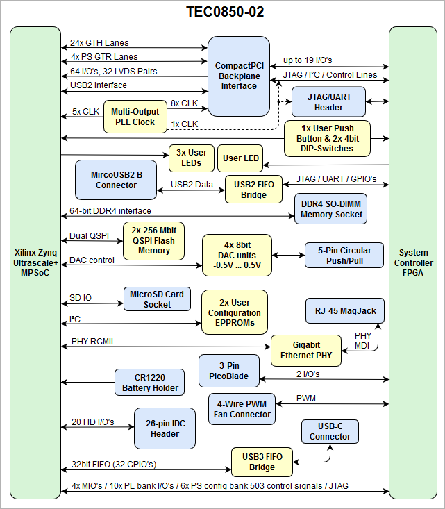
The Trenz Electronic TEC0850 board is a CompactPCI Serial card (3U form factor) integrating a Xilinx Zynq UltraScale+ MPSoC, one DDR4 SDRAM SODIMM socket with 64bit wide databusdata bus, max. dual 512 MByte Flash memory for configuration and operation, 24 Gigabit transceivers on PL side and 4 on PS side, powerful switch-mode power supplies for all on-board onboard voltages, USB2 and USB3 FIFO bridges and a large number of configurable I/Os available on the CompactPCI Serial backplane connectors.
Refer to http://trenz.org/tec0850-info for the current online version of this manual and other available documentation.
...
Zynq UltraScale+ MPSoC ZU15
- Front side interface connectors
- RJ-45 GbE Ethernet interface
- Circular push/pull connector with 4x on-board 8bit DAC output
- MicroSD Card connector
- USB2 and USB3 USB 2.0 and USB 3.0 to FIFO bridge connector
- 4x status LEDs
- 4 CompactPCI Serial connectors for backplane connection (3U form factor)
- 24 GTH lanes
- 4 PS GTR lanes
- USB2 USB 2.0 interface
- 64 Zynq PL HP I/O's
- 8x PLL clock input
- JTAG, I²C and 7 user I/O's to MAX10 FPGA
64bit DDR4 SODIMM (PS connected), 8 GByte maximum
Dual parallel QSPI Flash (bootable), 512 MByte maximum
- 26-pin header with 20 Zynq PL HD I/O's
- 3-pin header with 2 MAX10 FPGA I/O's
- System Controller (Altera MAX10 FPGA SoC)
- Power Sequencing
- System management and control for MPSoC and on-board onboard peripherals
- Si5345 programmable 10 output PLL clock generator
- Si53340 Quad clock buffer
- 2x 4bit DIP switches
- 1x user push button
- Zynq MPSoC cooling FAN connector
- On-board high-efficiency DC-DC converters
...
| Scroll Title | ||||||||||||||||||||||||||||||||||
|---|---|---|---|---|---|---|---|---|---|---|---|---|---|---|---|---|---|---|---|---|---|---|---|---|---|---|---|---|---|---|---|---|---|---|
| ||||||||||||||||||||||||||||||||||
|
Main Components
| Page properties | ||||
|---|---|---|---|---|
| ||||
Notes :
|
...
| Scroll Title | ||||||||||||||||||||||||||||||||||||
|---|---|---|---|---|---|---|---|---|---|---|---|---|---|---|---|---|---|---|---|---|---|---|---|---|---|---|---|---|---|---|---|---|---|---|---|---|
| ||||||||||||||||||||||||||||||||||||
|
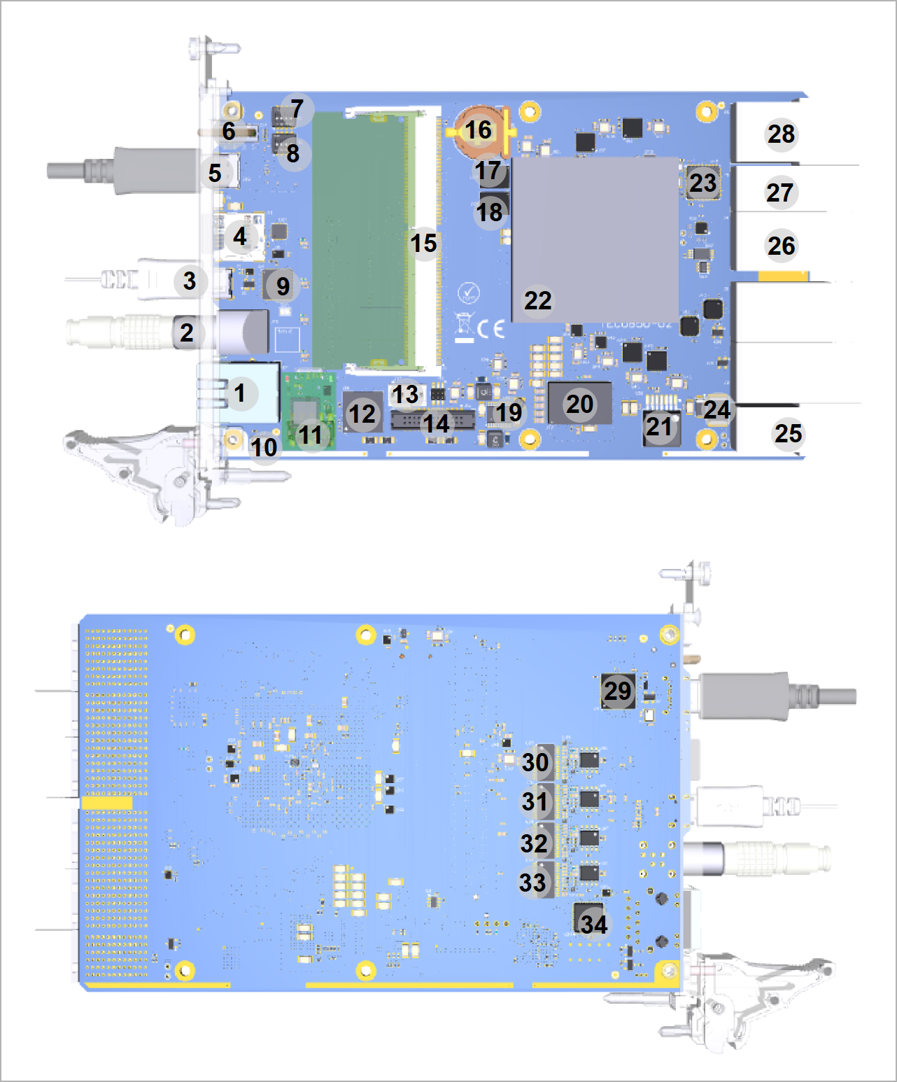
- GbE RJ-45 MagJack, J7
- 5-pin circular push/pull receptacle connector for DAC output, J15
- Micro USB2 USB 2.0 B receptacle connector, J9
- MicroSD Card socket, J11
- USB 3.0 Type C connector, J10
- LED light pipes J14 integrating LEDs D1 ... D4
- 4bit DIP-switch, S2
- 4bit DIP-switch, S1
- FTDI FT2232 USB2 to FIFO USB 2.0 to UART/JTAG bridge, U4
- 3-pin PicoBlade header, J8
- MAX10 FPGA JTAG/UART 10-pin header, J13
- Altera MAX10 System Controller FPGA, U18
- 4-Wire PWM fan connector, J17
- 26-pin IDC header for FPGA PL I/O's, J16
- DDR4 SO-DIMM 260-pin socket, U3
- Battery Holder CR1220, B1
- 256 Mbit (32 MByte) Micron Serial NOR Flash Memory N25Q256A, U24
- 256 Mbit (32 MByte) Micron Serial NOR Flash Memory N25Q256A, U25
- DC-DC Converter LT8471IFE @+5VA/-5VA, U74
- DC-DC Converter EM2130L02QI @VCCINT_0V85, U17
- DC-DC Converter 171050601 @5V, U50
- Xilinx Zynq Ultrascale+ MPSoC, U1
- Si5345A 10-output I²C programmable PLL clock, U14
- Main power fuse @2.5A/16V, F1
- cPCI connector, J1
- cPCI connector, J4
- cPCI connector, J5
- cPCI connector, J6
- FTDI FT601Q USB3 USB 3.0 to FIFO bridge, U9
- TI THS5641 8bit DAC ,U28
- TI THS5641 8bit DAC ,U31
- TI THS5641 8bit DAC ,U29
- TI THS5641 8bit DAC ,U33
- Marvell Alaska 88E1512 GbE PHY ,U20
Initial Delivery State
| Scroll Title | |||||||||||||||||||||||||||||||||
|---|---|---|---|---|---|---|---|---|---|---|---|---|---|---|---|---|---|---|---|---|---|---|---|---|---|---|---|---|---|---|---|---|---|
| |||||||||||||||||||||||||||||||||
|
...
| Page properties | ||||
|---|---|---|---|---|
| ||||
|
Signals, Interfaces and Pins
| Page properties | ||||
|---|---|---|---|---|
| ||||
Notes :
|
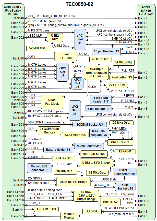
CompactPCI Backplane Connectors
The TEC0850 board is equipped with 3 CompactPCI high speed backplane connectors which provides serial high-speed interconnects with transmission rates up to 12 Gb/s to the Zynq MPSoCs MGT lanes, high speed USB2 interface and single ended FPGA I/O pins Zynq MPSoC and the System Controller FPGA.
The connectors support single ended and differential signaling as the Zynq MPSoC FPGA I/O's are routed from the FPGA banks as LVDS-pairs to the backplane connector.
The TEC0850 board is designed to be connected to the System Slot of the backplane connector, whereby 4 of the 6 connectors of the System Slot configuration are fitted to the TEC0850 board.
Following diagram gives an overview of the CompactPCI backplane connectors and their connections to the Zynq Ultrascale+ MPSoC and the System Controller FPGA U18:
...
| anchor | Figure_3 |
|---|---|
| title | Figure 3: TEC0850-02 CompactPCI I/O and high-speed interfaces |
To get started with TEC0850 board, some initial signals should be set described in the following table:
| Scroll Title | |||||||||||||||||||||||||||||||||||||||||||||||||||||||||||||||||||||||||||
|---|---|---|---|---|---|---|---|---|---|---|---|---|---|---|---|---|---|---|---|---|---|---|---|---|---|---|---|---|---|---|---|---|---|---|---|---|---|---|---|---|---|---|---|---|---|---|---|---|---|---|---|---|---|---|---|---|---|---|---|---|---|---|---|---|---|---|---|---|---|---|---|---|---|---|---|
| |||||||||||||||||||||||||||||||||||||||||||||||||||||||||||||||||||||||||||
|
Signals, Interfaces, and Pins
| Page properties | ||||
|---|---|---|---|---|
| ||||
Notes :
|
CompactPCI Serial Backplane Connectors
The TEC0850 board is equipped with 3 CompactPCI Serial high-speed backplane connectors which provide serial high-speed interconnects with transmission rates up to 12 Gb/s to the Zynq MPSoCs MGT lanes. On the cPCI connectors are also available single-ended Zynq MPSoC PL HP I/O's, high-speed USB 2.0 interface and single-ended I/O's of the System Controller FPGA.
The connectors support single-ended and differential signaling to the Zynq MPSoC PL HP banks 65 and 66 as those FPGA I/O's are routed as LVDS-pairs to the backplane connector.
The TEC0850 board is designed to be connected to the System Slot of the backplane, whereby 4 of the 6 connectors of the System Slot configuration are fitted to the TEC0850 board.
Following diagram gives an overview of the CompactPCI Serial backplane connectors and their connections to the Zynq Ultrascale+ MPSoC and the System Controller FPGA U18:
| Scroll Title | ||||||||||||||||||||||||||||||||
|---|---|---|---|---|---|---|---|---|---|---|---|---|---|---|---|---|---|---|---|---|---|---|---|---|---|---|---|---|---|---|---|---|
| ||||||||||||||||||||||||||||||||
|
Following tables contains information about the interfaces, I/O's, clock and VCCIO sources available on the cPCI connectors:
- CompactPCI Serial Connector J1
- CompactPCI Serial Connector J3
- CompactPCI Serial Connector J4
- CompactPCI Serial Connector J5
- CompactPCI Serial Connector J6
Anchor CompactPCI Connector J1 CompactPCI Connector J1
CompactPCI Serial Connector J1
| Scroll Title | |||||||||||||||||||||||||||||||||||||||||||||||||||||||||||||||||
|---|---|---|---|---|---|---|---|---|---|---|---|---|---|---|---|---|---|---|---|---|---|---|---|---|---|---|---|---|---|---|---|---|---|---|---|---|---|---|---|---|---|---|---|---|---|---|---|---|---|---|---|---|---|---|---|---|---|---|---|---|---|---|---|---|---|
| |||||||||||||||||||||||||||||||||||||||||||||||||||||||||||||||||
|
| Scroll Title | ||||
|---|---|---|---|---|
|
...
| Scroll Only |
|---|
|
Following tables contains information about the interfaces, I/O's, clock and VCCIO sources available on the cPCI connectors:
...
CompactPCI Connector J1
| Scroll Title | |||||||||||||||||||||||||||||||
|---|---|---|---|---|---|---|---|---|---|---|---|---|---|---|---|---|---|---|---|---|---|---|---|---|---|---|---|---|---|---|---|
| |||||||||||||||||||||||||||||||
| Scroll Table Layout | |||||||||||||||||||||||||||||||
| orientation | portrait | ||||||||||||||||||||||||||||||
| sortDirection | ASC | ||||||||||||||||||||||||||||||
| repeatTableHeaders | default | style | widths | ||||||||||||||||||||||||||||
| sortByColumn | 1 | ||||||||||||||||||||||||||||||
| sortEnabled | false | ||||||||||||||||||||||||||||||
| cellHighlighting | true | ||||||||||||||||||||||||||||||
| Interfaces | I/O Signal Count | LVDS-pairs count | Connected to | VCCO bank Voltage | Notes | ||||||||||||||||||||||||||
| I/O | 1 | - | SC FPGA U18 Bank 6 | +3V_D | control signals in cPCI pin assingment | ||||||||||||||||||||||||||
| 6 | - | SC FPGA U18 Bank 8 | +3V_D | control signals in cPCI pin assingment | |||||||||||||||||||||||||||
| I²C | 2 | - | SC FPGA U18 Bank 1A | +3V_D | SC FPGA U18 I²C interface | ||||||||||||||||||||||||||
| JTAG | 4 | - | SC FPGA U18 Bank 1A | +3V_D | SC FPGA U18 JTAG interface | ||||||||||||||||||||||||||
| MGT | - | 8 (4 x RX/TX) | Bank 502 PS GTR | - | 4x PS GTR lanes | ||||||||||||||||||||||||||
| USB2 | - | 1 (RX/TX) | USB2 PHY U11 | - | USB2 OTG A-Device (host) | ||||||||||||||||||||||||||
| Clock Input | - | 1 | Clock Driver U73 | - | 1x Reference clock input from PLL clock U14 | ||||||||||||||||||||||||||
| Scroll Title | |||||||||||||||||||||||||||||||
| |||||||||||||||||||||||||||||||
| Scroll Table Layout | |||||||||||||||||||||||||||||||
| orientation | portrait | ||||||||||||||||||||||||||||||
| sortDirection | ASC | ||||||||||||||||||||||||||||||
| repeatTableHeaders | default | style | widths | ||||||||||||||||||||||||||||
| sortByColumn | 1 | ||||||||||||||||||||||||||||||
| sortEnabled | false | ||||||||||||||||||||||||||||||
| cellHighlighting | true | ||||||||||||||||||||||||||||||
| MGT Lane | Bank | Type | Signal Schematic Name | cPCI Connector Pin | FPGA Pin | ||||||||||||||||||||||||||
| 0 | 505 | GTR |
| J1-D5 | PS_MGTRRXP0_505, AB29 | ||||||||||||||||||||||||||
| 1 | 505 | GTR |
| J1-J5 | PS_MGTRRXP1_505, Y29 | ||||||||||||||||||||||||||
| 2 | 505 | GTR |
| J1-E6 | PS_MGTRRXP2_505, W31 | ||||||||||||||||||||||||||
| 3 | 505 | GTR |
| J1-K6 | PS_MGTRRXP3_505, V29 | ||||||||||||||||||||||||||
| Scroll Title | |||||||||||||||||||||||||||||||
| |||||||||||||||||||||||||||||||
| |||||||||||||||||||||||||||||||
| Scroll Title | |||||||||||||||||||||||||||||||
| |||||||||||||||||||||||||||||||
| Scroll Table Layout | |||||||||||||||||||||||||||||||
| orientation | portrait | ||||||||||||||||||||||||||||||
| sortDirection | ASC | ||||||||||||||||||||||||||||||
| repeatTableHeaders | default | style | widths | ||||||||||||||||||||||||||||
| sortByColumn | 1 | ||||||||||||||||||||||||||||||
| sortEnabled | false | ||||||||||||||||||||||||||||||
| cellHighlighting | true | ||||||||||||||||||||||||||||||
| Available VCC/VCCIO | cPCI Connector Pin | Source | Notes | VIN_12V | J1-A1 | cPCI backplanemin. cur.: 6.65A |
...
CompactPCI Connector J4
...
| anchor | Table_6 |
|---|---|
| title | Table 6: cPCI J4 MGT lanes |
...
- PE3_RX0_P
- PE3_RX0_N
- PE3_TX0_P
- PE3_TX0_N
...
J4-D1
J4-E1
J4-A1
J4-B1
...
MGTHRXP0_128, T33
MGTHRXN0_128, T34
MGTHTXP0_128, T29
MGTHTXN0_128, T30
...
- PE3_RX1_P
- PE3_RX1_N
- PE3_TX1_P
- PE3_TX1_N
...
J4-J1
J4-K1
J4-G1
J4-H1
...
MGTHRXP1_128, P33
MGTHRXN1_128, P34
MGTHTXP1_128, R31
MGTHTXN1_128, R32
...
- PE3_RX2_P
- PE3_RX2_N
- PE3_TX2_P
- PE3_TX2_N
...
J4-E2
J4-F2
J4-B2
J4-C2
...
MGTHRXP2_128, N31
MGTHRXN2_128, N32
MGTHTXP2_128, P29
MGTHTXN2_128, P30
...
- PE3_RX3_P
- PE3_RX3_N
- PE3_TX3_P
- PE3_TX3_N
...
J4-K2
J4-L2
J4-H2
J4-I2
...
MGTHRXP3_128, M33
MGTHRXN3_128, M34
MGTHTXP3_128, M29
MGTHTXN3_128, M30
...
- PE4_RX0_P
- PE4_RX0_N
- PE4_TX0_P
- PE4_TX0_N
...
J4-D3
J4-E3
J4-A3
J4-B3
...
MGTHRXP0_129, L31
MGTHRXN0_129, L32
MGTHTXP0_129, K29
MGTHTXN0_129, K30
...
- PE4_RX1_P
- PE4_RX1_N
- PE4_TX1_P
- PE4_TX1_N
...
J4-J3
J4-K3
J4-G3
J4-H3
...
MGTHRXP1_129, K33
MGTHRXN1_129, K34
MGTHTXP1_129, J31
MGTHTXN1_129, J32
...
- PE4_RX2_P
- PE4_RX2_N
- PE4_TX2_P
- PE4_TX2_N
...
J4-E4
J4-F4
J4-B4
J4-C4
...
MGTHRXP2_129, H33
MGTHRXN2_129, H34
MGTHTXP2_129, H29
MGTHTXN2_129, H30
...
- PE4_RX3_P
- PE4_RX3_N
- PE4_TX3_P
- PE4_TX3_N
...
J4-K4
J4-L4
J4-H4
J4-I4
...
MGTHRXP3_129, F33
MGTHRXN3_129, F34
MGTHTXP3_129, G31
MGTHTXN3_129, G32
...
- PE5_RX0_P
- PE5_RX0_N
- PE5_TX0_P
- PE5_TX0_N
...
J4-D5
J4-E5
J4-A5
J4-B5
...
MGTHRXP3_130, B33
MGTHRXN3_130, B34
MGTHTXP3_130, A31
MGTHTXN3_130, A32
...
- PE5_RX1_P
- PE5_RX1_N
- PE5_TX1_P
- PE5_TX1_N
...
J4-J5
J4-K5
J4-G5
J4-H5
...
MGTHRXP2_130, C31
MGTHRXN2_130, C32
MGTHTXP2_130, B29
MGTHTXN2_130, B30
...
- PE5_RX2_P
- PE5_RX2_N
- PE5_TX2_P
- PE5_TX2_N
...
J4-E6
J4-F6
J4-B6
J4-C6
...
MGTHRXP1_130, D33
MGTHRXN1_130, D34
MGTHTXP1_130, D29
MGTHTXN1_130, D30
...
- PE5_RX3_P
- PE5_RX3_N
- PE5_TX3_P
- PE5_TX3_N
...
J4-K6
J4-L6
J4-H6
J4-I6
...
MGTHRXP0_130, E31
MGTHRXN0_130, E32
MGTHTXP0_130, F29
MGTHTXN0_130, F30
...
- PE6_RX0_P
- PE6_RX0_N
- PE6_TX0_P
- PE6_TX0_N
...
J4-D7
J4-E7
J4-A7
J4-B7
...
MGTHRXP3_230, A4
MGTHRXN3_230, A3
MGTHTXP3_230, A8
MGTHTXN3_230, A7
...
- PE6_RX1_P
- PE6_RX1_N
- PE6_TX1_P
- PE6_TX1_N
...
J4-J7
J4-K7
J4-G7
J4-H7
...
MGTHRXP2_230, B2
MGTHRXN2_230, B1
MGTHTXP2_230, B6
MGTHTXN2_230, B5
...
- PE6_RX2_P
- PE6_RX2_N
- PE6_TX2_P
- PE6_TX2_N
...
J4-E8
J4-F8
J4-B8
J4-C8
...
MGTHRXP1_230, C4
MGTHRXN1_230, C3
MGTHTXP1_230, D6
MGTHTXN1_230, D5
...
- PE6_RX3_P
- PE6_RX3_N
- PE6_TX3_P
- PE6_TX3_N
...
J4-K8
J4-L8
J4-H8
J4-I8
...
MGTHRXP0_230, D2
MGTHRXN0_230, D1
MGTHTXP0_230, E4
MGTHTXN0_230, E3
...
CompactPCI Connector J5
...
| anchor | Table_7 |
|---|---|
| title | Table 7: cPCI J5 MGT lanes |
...
- PE8_RX0_P
- PE8_RX0_N
- PE8_TX0_P
- PE8_TX0_N
...
J5-D3
J5-E3
J5-A3
J5-B3
...
MGTHRXP0_228, T2
MGTHRXN0_228, T1
MGTHTXP0_228, R4
MGTHTXN0_228, R3
...
- PE8_RX1_P
- PE8_RX1_N
- PE8_TX1_P
- PE8_TX1_N
...
J5-J3
J5-K3
J5-G3
J5-H3
...
MGTHRXP1_228, P2
MGTHRXN1_228, P1
MGTHTXP1_228, P6
MGTHTXN1_228, P5
...
- PE8_RX2_P
- PE8_RX2_N
- PE8_TX2_P
- PE8_TX2_N
...
J5-E4
J5-F4
J5-B4
J5-C4
...
MGTHRXP2_228, M2
MGTHRXN2_228, M1
MGTHTXP2_228, N4
MGTHTXN2_228, N3
...
- PE8_RX3_P
- PE8_RX3_N
- PE8_TX3_P
- PE8_TX3_N
...
J5-K4
J5-L4
J5-H4
J5-I4
...
MGTHRXP3_228, L4
MGTHRXN3_228, L3
MGTHTXP3_228, M6
MGTHTXN3_228, M5
...
- PE7_RX0_P
- PE7_RX0_N
- PE7_TX0_P
- PE7_TX0_N
...
J5-D1
J5-E1
J5-A1
J5-B1
...
MGTHRXP0_229, K2
MGTHRXN0_229, K1
MGTHTXP0_229, K6
MGTHTXN0_229, K5
...
- PE7_RX1_P
- PE7_RX1_N
- PE7_TX1_P
- PE7_TX1_N
...
J5-J1
J5-K1
J5-G1
J5-H1
...
MGTHRXP1_229, J4
MGTHRXN1_229, J3
MGTHTXP1_229, H6
MGTHTXN1_229, H5
...
- PE7_RX2_P
- PE7_RX2_N
- PE7_TX2_P
- PE7_TX2_N
...
J5-E2
J5-F2
J5-B2
J5-C2
...
MGTHRXP2_229, H2
MGTHRXN2_229, H1
MGTHTXP2_229, G4
MGTHTXN2_229, G3
...
- PE7_RX3_P
- PE7_RX3_N
- PE7_TX3_P
- PE7_TX3_N
...
J5-K2
J5-L2
J5-H2
J5-I2
...
MGTHRXP3_229, F2
MGTHRXN3_229, F1
MGTHTXP3_229, F6
MGTHTXN3_229, F5
|
| Scroll Title | ||||||||||||||||||||||||||||
|---|---|---|---|---|---|---|---|---|---|---|---|---|---|---|---|---|---|---|---|---|---|---|---|---|---|---|---|---|
| ||||||||||||||||||||||||||||
|
| Anchor | ||||
|---|---|---|---|---|
|
CompactPCI Serial Connector J3
CompactPCI Serial connector J3 is not fitted on the TEC0850 board by default, but is necessary if the second optional USB2 PHY U13 if fitted and its USB2 differential serial data interface is connected to the cPCI connector J2.
| Scroll Title | ||||||||||||||||||||||||||||||
|---|---|---|---|---|---|---|---|---|---|---|---|---|---|---|---|---|---|---|---|---|---|---|---|---|---|---|---|---|---|---|
| ||||||||||||||||||||||||||||||
|
| Anchor | ||||
|---|---|---|---|---|
|
CompactPCI Serial Connector J4
| Scroll Title | ||||||||||||||||||||||||||||||||||||||||||||||||||||||||||||||||||||||||||||||||||||||||||||||||||||||||||||||||||||||||
|---|---|---|---|---|---|---|---|---|---|---|---|---|---|---|---|---|---|---|---|---|---|---|---|---|---|---|---|---|---|---|---|---|---|---|---|---|---|---|---|---|---|---|---|---|---|---|---|---|---|---|---|---|---|---|---|---|---|---|---|---|---|---|---|---|---|---|---|---|---|---|---|---|---|---|---|---|---|---|---|---|---|---|---|---|---|---|---|---|---|---|---|---|---|---|---|---|---|---|---|---|---|---|---|---|---|---|---|---|---|---|---|---|---|---|---|---|---|---|---|---|
| ||||||||||||||||||||||||||||||||||||||||||||||||||||||||||||||||||||||||||||||||||||||||||||||||||||||||||||||||||||||||
|
Anchor CompactPCI Connector J5 CompactPCI Connector J5
CompactPCI Serial Connector J5
| Scroll Title | ||||||||||||||||||||||||||||||||||||||||||||||||||||||||||||||||||||||||
|---|---|---|---|---|---|---|---|---|---|---|---|---|---|---|---|---|---|---|---|---|---|---|---|---|---|---|---|---|---|---|---|---|---|---|---|---|---|---|---|---|---|---|---|---|---|---|---|---|---|---|---|---|---|---|---|---|---|---|---|---|---|---|---|---|---|---|---|---|---|---|---|---|
| ||||||||||||||||||||||||||||||||||||||||||||||||||||||||||||||||||||||||
|
| Scroll Title | ||||
|---|---|---|---|---|
|
...
| anchor | Table_8 |
|---|---|
| title | Table 8: cPCI J5 clock signals: |
...
- PE1_CLK_P
- PE1_CLK_N
...
J5-A5
J5-B5
...
reference clock signals supplied
by on-board 10-output
PLL clock generator U14
...
- PE2_CLK_P
- PE2_CLK_N
...
J5-D5
J5-E5
...
- PE3_CLK_P
- PE3_CLK_N
...
J5-G5
J5-H5
...
- PE4_CLK_P
- PE4_CLK_N
...
J5-J5
J5-K5
...
- PE5_CLK_P
- PE5_CLK_N
...
J5-B6
J5-C6
...
- PE6_CLK_P
- PE6_CLK_N
...
J5-E6
J5-F6
...
- PE7_CLK_P
- PE7_CLK_N
...
J5-H6
J5-I6
...
- PE8_CLK_P
- PE8_CLK_N
...
J5-K6
J5-L6
...
CompactPCI Connector J6
| Scroll Title | ||||||||||||||||||
|---|---|---|---|---|---|---|---|---|---|---|---|---|---|---|---|---|---|---|
| ||||||||||||||||||
| ||||||||||||||||||
| Interfaces | I/O Signal Count | LVDS-pairs count | Connected to | VCCO bank Voltage | Notes | |||||||||||||
| I/O | 46 | 23 | PL bank 66 | PL_1.8V | - | |||||||||||||
| 18 | 9 | PL bank 65 | PL_1.8V | - | ||||||||||||||
| 2 | - | SC FPGA U18 Bank 1B | +3V_D | Signalname: 'DET_RIO', 'DET_BPR' |
USB-C Connector
Front panel USB-C Interface is connected to USB FIFO bridge chip FT601Q. 32-bit FIFO bridge provides a simple high-speed interface to Zynq UltraScale+ PL.
...
| anchor | Figure_4 |
|---|---|
| title | Figure 4: TEC0850-02 USB3 to FIFO bridge |
|
Anchor CompactPCI Connector J6 CompactPCI Connector J6
CompactPCI Serial Connector J6
| Scroll Title | ||||
|---|---|---|---|---|
|
...
| Scroll Only |
|---|
|
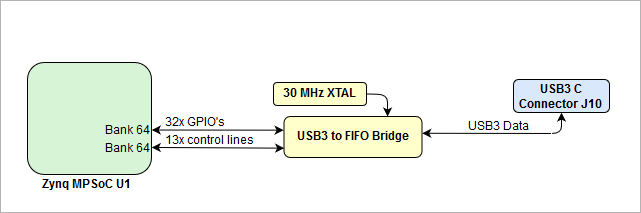
The USB3 to FIFO bridge FTDI FT601Q U9 is connected to the Zynq MPSoC's PL bank 64 and is accessible through USB-C connector J10:
| Scroll Title | ||||||||||||||||||||||||||||||||||||||||
|---|---|---|---|---|---|---|---|---|---|---|---|---|---|---|---|---|---|---|---|---|---|---|---|---|---|---|---|---|---|---|---|---|---|---|---|---|---|---|---|---|
| ||||||||||||||||||||||||||||||||||||||||
|
See FT600Q-FT601Q IC Datasheet for interface details.
Micro-USB2 Connector
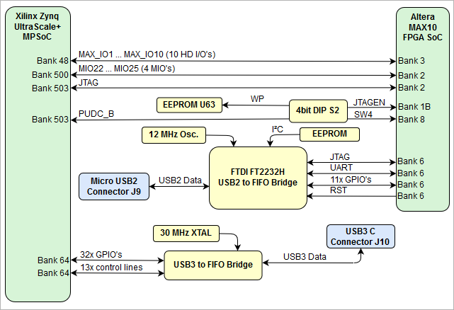
Front panel Micro-USB2 Interface provides access to UART and JTAG functions via FTDI FT2232 chip. Use of this feature requires that USB driver is installed on your host PC. UART0 with MIO 22 .. 23 should be selected in "Zynq UltraScale+ MPSoC" configuration.
The Digilent plug-in software and cable drivers must be installed on your machine for you to be able to use JTAG interface.
|
USB-C Connector
Front panel USB-C Interface is connected to USB FIFO bridge chip FT601Q. 32-bit FIFO bridge provides a simple high-speed interface to Zynq UltraScale+ PL.
| Scroll Title | ||||||||||||||||||||||||||||
|---|---|---|---|---|---|---|---|---|---|---|---|---|---|---|---|---|---|---|---|---|---|---|---|---|---|---|---|---|
| ||||||||||||||||||||||||||||
| ||||||||||||||||||||||||||||
| Scroll Title | ||||||||||||||||||||||||||||
| ||||||||||||||||||||||||||||
|
The USB2 The USB 3.0 to FIFO bridge FTDI FT2232H U4 FT601Q U9 is connected to the SC FPGA U18 Zynq MPSoC's PL bank 64 and is accessible through MicroUSB-USB2 C connector J9J10:
| Scroll Title | ||||||||||||||||||||||||||||||||||
|---|---|---|---|---|---|---|---|---|---|---|---|---|---|---|---|---|---|---|---|---|---|---|---|---|---|---|---|---|---|---|---|---|---|---|
| ||||||||||||||||||||||||||||||||||
|
SD
|
See FT600Q-FT601Q IC Datasheet for interface details.
Micro-USB2 Connector
Front panel Micro-USB2 Interface provides access to UART and JTAG functions via FTDI FT2232 chip. Use of this feature requires that USB driver is installed on your host PC. UART0 with MIO 22 .. 23 should be selected in "Zynq UltraScale+ MPSoC" configuration.
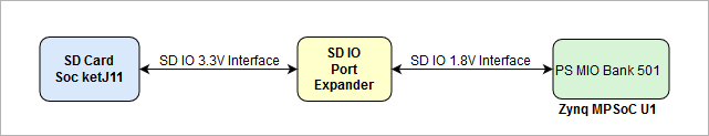
The Digilent plug-in software and cable drivers must be installed on your machine for you to be able to use JTAG interfaceThe SD Card interface of the TEC0850 board is not directly wired to the connector J11 pins, but through a Texas Instruments TXS02612 SD IO Port Expander, which is needed for voltage translation due to different voltage levels of the Micro SD Card and MIO-bank of the Xilinx Zynq MPSoC. The Micro SD Card has 3.3V signal voltage level, but the PS MIO-bank on the Xilinx Zynq MPSoC has VCCIO of 1.8V.
| Scroll Title | ||||||||||||||||||||||||||||||||
|---|---|---|---|---|---|---|---|---|---|---|---|---|---|---|---|---|---|---|---|---|---|---|---|---|---|---|---|---|---|---|---|---|
| ||||||||||||||||||||||||||||||||
|
The USB2 to FIFO bridge FTDI FT2232H U4 is connected to the SC FPGA U18 and is accessible through Micro-USB2 connector J9:
| scroll- |
|---|
| title |
|
There are some limitations to use SD card Interface in Linux.
- Zynq UltraScale+ SD controller is working only in the 3.3V mode as it connected to SD card socket using SD IO port expander U10 as 1.8V to 3.3V level shifter.
- Micro SD card socket has no "Write Protect" switch.
| Tip |
|---|
To force Linux driver not to use this features add following instructions to device tree file. &sdhci1 { no-1-8-v; |
RJ45 - Ethernet
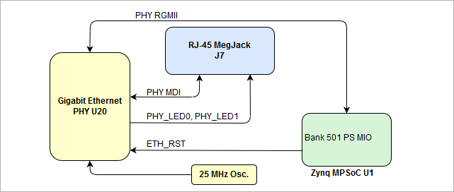
On-board Gigabit Ethernet PHY is provided with Marvell Alaska 88E1512 IC U20. The Ethernet PHY RGMII interface is connected to the Zynq MPSoC Ethernet interface of the PS MIO bank 501. I/O voltage is fixed at 1.8V for HSTL signaling. The reference clock input of the PHY is supplied from the on-board 25.000000 MHz oscillator U21. The LEDs of the RJ-45 MegJack J13 are connected to the GbE PHY U20 status LED output.
...
| anchor | Figure_7 |
|---|---|
| title | Figure 7: Gigabit Ethernet Interface |
| ||||||||||||||||||||||||||||||||||
|
SD
The SD Card interface of the TEC0850 board is not directly wired to the connector J11 pins but through a Texas Instruments TXS02612 SD IO Port Expander, which is needed for voltage translation due to different voltage levels of the Micro SD Card and MIO-bank of the Xilinx Zynq MPSoC. The Micro SD Card has 3.3V signal voltage level, but the PS MIO-bank on the Xilinx Zynq MPSoC has VCCIO of 1.8V
...
| Scroll Only |
|---|
|
DDR4 SODIMM Socket
On the TEC0850 board there is a DDR4 memory interface U3 with a 64-bit databus width available for SO-DIMM modules connected to the Zynq UltraScale+ DDRC hard memory controller.
| Scroll Title | ||||||||||||||||||||||||||||||||||
|---|---|---|---|---|---|---|---|---|---|---|---|---|---|---|---|---|---|---|---|---|---|---|---|---|---|---|---|---|---|---|---|---|---|---|
| ||||||||||||||||||||||||||||||||||
|
...
There are some limitations to use SD card Interface in Linux.
- Zynq UltraScale+ SD controller is working only in the 3.3V mode as it connected to SD card socket using SD IO port expander U10 as 1.8V to 3.3V level shifter.
- Micro SD card socket has no "Write Protect" switch.
| Tip |
|---|
To force Linux driver not to use these features to add following instructions to device tree file. &sdhci1 { no-1-8-v; |
RJ45 - Ethernet
Onboard Gigabit Ethernet PHY is provided with Marvell Alaska 88E1512 IC U20. The Ethernet PHY RGMII interface is connected to the Zynq MPSoC Ethernet interface of the PS MIO bank 501. I/O voltage is fixed at 1.8V for HSTL signaling. The reference clock input of the PHY is supplied from the on-board 25.000000 MHz oscillator U21. The LEDs of the RJ-45 MegJack J13 are connected to the GbE PHY U20 status LED output.
| Scroll Title | ||||||||||||||||||||||||||||||||
|---|---|---|---|---|---|---|---|---|---|---|---|---|---|---|---|---|---|---|---|---|---|---|---|---|---|---|---|---|---|---|---|---|
| ||||||||||||||||||||||||||||||||
|
DDR4 SODIMM Socket
On the TEC0850 board, there is a DDR4 memory interface U3 with a 64-bit data bus width available for SO-DIMM modules connected to the Zynq UltraScale+ DDRC hard memory controller.
| Scroll Title | ||||||||||||||||||||||||||||||||
|---|---|---|---|---|---|---|---|---|---|---|---|---|---|---|---|---|---|---|---|---|---|---|---|---|---|---|---|---|---|---|---|---|
| ||||||||||||||||||||||||||||||||
|
Following table gives an overview of the memory interface I/O signals of the DDR4 SDRAM SO-DIMM Socket U3:
| Scroll Title | |||||||||||||||||||||||||||||||||||||||||||||||||||||||||||||||||||||||
|---|---|---|---|---|---|---|---|---|---|---|---|---|---|---|---|---|---|---|---|---|---|---|---|---|---|---|---|---|---|---|---|---|---|---|---|---|---|---|---|---|---|---|---|---|---|---|---|---|---|---|---|---|---|---|---|---|---|---|---|---|---|---|---|---|---|---|---|---|---|---|---|
| |||||||||||||||||||||||||||||||||||||||||||||||||||||||||||||||||||||||
|
Circular Push Pull Connector
The TEC0850 board provides 4x DAC analog voltage output on the 5-pin circular push/pull connector J15. Each of the DAC units consists of one Texas Instruments THS5641AIPW digital to analog converter, TI THS4631D operational amplifier and two LDOs, by which the DAC unit can be switched on and off.
The TI THS4631D digital to analog converter wired to the operational amplifier circuitry creating the DAC unit with a voltage output range from -0.5V ... 0.5V. See TI THS5641 datasheet and schematic how to control the DAC unit and to set the analog output voltages on connector J15.
| Scroll Title | ||||
|---|---|---|---|---|
| ||||
|
...
| anchor | Table_12 |
|---|---|
| title | Table 12: DDR4 SDRAM SO-DIMM socket U3 |
...
Signal Schematic Name
...
- DDR4-A0 ... DDR4-A16
...
- DDR4-BA0 / DDR4-BA1
...
- DDR4-BG0 / DDR4-BG1
...
- DDR4-CLK0_P
- DDR4-CLK0_N
- DDR4-CLK1_P
- DDR4-CLK1_N
...
- DQ0 ... DQ63
...
- CB0 ... CB7
...
- DDR4-DQS0_P
- DDR4-DQS0_N
- ...
- DDR4-DQS8_P
- DDR4-DQS8_N
...
- DDR4-DM0 ... DDR4-DM8
...
- DDR4-SA0 ... DDR4-SA2
...
address range configuration on I²C bus
...
- DDR4-CS_N0 / DDR4-CS_N1
...
- DDR4-ODT0 / DDR4-ODT1
...
- DDR4-RESET
...
- DDR4-PAR
...
- DDR4-CKE0 / DDR4-CKE1
...
- DDR4-ALERT
...
- DDR4-ACT
...
- DDR4-EVENT
...
- DDR4-SCL
- DDR4-SDA
...
Circular Push Pull Connector
The TEC0850 board provides 4x DAC analog voltage output on the 5-pin circular push/pull connector J15. Each of the DAC units consists of one Texas Instruments THS5641AIPW digital to analog converter, TI THS4631D operational amplifier and two LDOs, by which the DAC unit can be switched on and off.
The TI THS4631D digital to analog converter wired to the operational amplifier circuitry creating the DAC unit with a voltage output range from -0.5V ... 0.5V. See TI THS5641 datasheet and schematic how to control the DAC unit and to set the analog output voltages on connector J15.
...
| anchor | Figure_9 |
|---|---|
| title | Figure 9: 4x 8bit DAC units |
...
26-Pin IDC Header
There is a 26-pin IDC header (2x13, 1.27mm grid size) J16 available on the TEC0850 board which exposes the 20 FPGA HD I/O's of PL bank 47 to the user. The PL bank 47 has 3.3V VCCO bank voltage, on the header J16 there also the voltage levels 3.3V and 5V available. The I/O's can be accessed with a corresponding IDC connector.
...
| anchor | Figure_10 |
|---|---|
| title | Figure 10: Zynq MPSoC PL I/O's IDC pin-header |
...
10-Pin Header
On the TEC0850 there is a 10-pin SMT header (2x5, 2.54mm grid size) J13 present which provides access to the JTAG and UART interface of Altera MAX10 System Controller FPGA. The header J13 has a compatible pin assignment to the TEI0004 JTAG programmer for Altera FPGAs, the voltage levels 3.3V is on the header available as reference I/O-voltage for JTAG and UART.
The 4 JTAG pins of the header J13 are also connected to the cPCI connector J1 and can be used es user GPIO's of the SC FPGA U18 with othr functionalities then JTAG.
On the header J13 there is also a reference clock signal from PLL clcok U14 available, which can be also used for the SC FPGA U18 and on the cPCI connector J1.
| Scroll Title | ||||||||||||||||||||||||||||
|---|---|---|---|---|---|---|---|---|---|---|---|---|---|---|---|---|---|---|---|---|---|---|---|---|---|---|---|---|
| anchor | Figure_11 | title | Figure 11: 10-pin JTAG/UART header
|
...
26-Pin
...
IDC Header
There is a 26-pin IDC header (2x13, 1.27mm grid size) J16 available on the TEC0850 board which exposes the 20 FPGA HD 2 I/O's of the SC FPGA U18 are exposed to the on-board 3-Pin PicoBlade header J8 available to the user or for future use of upcoming versions of SC FPGA firmware.PL bank 47 to the user. The PL bank 47 has 3.3V VCCO bank voltage, on the header J16 there also the voltage levels 3.3V and 5V available. The I/O's can be accessed with a corresponding IDC connector.
| Scroll Title | ||||||||||||||||||||||||
|---|---|---|---|---|---|---|---|---|---|---|---|---|---|---|---|---|---|---|---|---|---|---|---|---|
| ||||||||||||||||||||||||
|

Battery Holder
There is a CR1220 battery holder available to the supply the voltage for the for for the Zynq MPSoC's Battery Power Domain (BBRAM and RTC). The battery voltage VBATT should be in the range of 2.2V to 5.5V, use 3.0V CR1220 battery.
| |||||||||||||||||||||||||||
| Scroll Title | |||||||||||||||||||||||||||
|---|---|---|---|---|---|---|---|---|---|---|---|---|---|---|---|---|---|---|---|---|---|---|---|---|---|---|---|
| |||||||||||||||||||||||||||
|
10-
...
Pin Header
On the TEC0850 there is a 10-pin SMT header (2x5, 2.54mm grid size) J13 present which provides access to the JTAG and UART interface of Altera MAX10 System Controller FPGA. The header J13 has a compatible pin assignment to the TEI0004 JTAG programmer for Altera FPGAs, the voltage levels 3.3V is on the header available as a reference I/O-voltage for JTAG and UART.
The 4 JTAG pins of the header J13 are also connected to the cPCI connector J1 and can be used as user GPIO's of the SC FPGA U18 with other functionalities then JTAG.
On the header J13, there is also a optional reference clock signal from PLL clock U14 available, if the necessary resistors and capacitors are fitted on board. The clock can also be used for the SC FPGA U18 and on the cPCI connector J1.
| Scroll Title | ||||
|---|---|---|---|---|
| ||||
|
4-Wire PWM FAN Connectors
The TEC0850 offers one 4-wire PWM FAN connector FPGA cooling fan controlled by SC FPGA U18:
| Scroll Title | ||||||||||||||||||||||||||||
|---|---|---|---|---|---|---|---|---|---|---|---|---|---|---|---|---|---|---|---|---|---|---|---|---|---|---|---|---|
| anchor | Figure_14 | title | Figure 14: 4-wire PWM FAN connector
|
3-
...

On-board Peripherals
| Page properties | ||||
|---|---|---|---|---|
| ||||
Notes :
|
Zynq UltraScale XCZU15EG MPSoC
The TEC0850 board is populated with the Zynq UltraScale+ XCZU15EG-1FFVB1156E MPSoC.
The PS MIO pins are routed to the on-board peripherals as follows:
...
| anchor | Table_13 |
|---|---|
| title | Table 13: Default MIO Configuration |
...
MAX10 System Controller FPGA
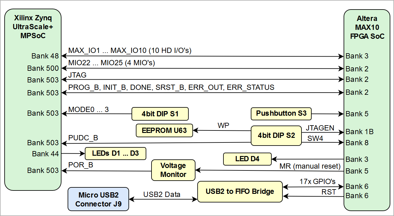
The TEC0850 board is equipped with one System Controller FPGA (Intel MAX10 10M08SAU169C8G) with the schematic designators U18. The SC FPGA is the central system management unit where essential control signals are logically linked by the implemented logic in FPGA firmware, which generates output signals to control the system, the on-board peripherals and the interfaces. Interfaces like JTAG and UART between the FTDI FT2232H chip and to the Zynq MPSoC are by-passed, forwarded and controlled by the System Controller FPGA.
Other tasks of the System Controller FPGA are the monitoring of the power-on sequence and to display the programming state of the FPGA module. The functionalities and configuration of the pins depend on the SC FPGA's firmware. The documentation of the firmware of SC FPGA U18 contains detailed information on this matter.
The Sytem Controller FPGA is connected to the Zynq Ultrascale+ MPSoC through MIO and PL pins. The signals of these pins are forwarded by the SC FPGA to control some of the on board peripherals.
Following block diagram visualizes the connection of the SC FPGA with the Zynq Ultrascale+ MPSoC via 4 PS MIO pins (MIO22 ... 25), PS Config control signals and 10 singled ended PL HD bank 48 I/O pins (MAX_IO1 ... MAX_IO10):
...
| anchor | Figure_2 |
|---|---|
| title | Figure 2: TEF1001-02 main components |
...
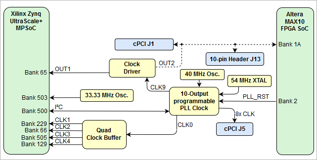
Programmable Clock Generator
There is a Si5345A U14, Silicon Labs I2C programmable 10-output PLL clock generator on-board to generate various reference clocks for the Zynq MPSoC MGT banks and on-board peripherals.
...
| anchor | Figure_2 |
|---|---|
| title | Figure 2: TEF1001-02 main components |
...
Following table shows on-board Silicon Labs I2C programmable Si5345A U17 10-output programmable PLL reference clock generator inputs and outputs:
...
| anchor | Table_x |
|---|---|
| title | Table x: SI5345 I2C address |
...
- IN0_P
...
- IN0_N
...
-
...
-
...
not used
...
- CLK0_P
...
reference clock input to
Quad clock buffer
...
- CLK0_N
...
- PE1_CLK_N
...
reference clock output
to cPCI connector J5
...
- PE1_CLK_P
...
- PE5_CLK_N
...
- PE5_CLK_P
...
- PE2_CLK_N
...
- PE2_CLK_P
...
- PE3_CLK_N
...
- PE3_CLK_P
...
- PE4_CLK_N
...
- PE4_CLK_P
...
- PE6_CLK_N
...
- PE6_CLK_P
...
- PE8_CLK_N
...
- PE8_CLK_P
...
- PE7_CLK_N
...
- PE7_CLK_P
...
- CLK9_P
...
reference clock input to
dual clock driver
...
- CLK9_N
...
- XAXB_P
...
- XAXB_N
...
SCLK,
SDA/SDIO
...
- I2C_SCL
- I2C_SDA
...
- MIO20
- MIO21
...
| anchor | Table_x |
|---|---|
| title | Table x: SI5345 I2C address |
...
- CLK1_P
- CLK1_N
...
U1, pin G8
U1, pin G7
...
- CLK2_P
- CLK2_N
...
U1, pin Y8
U1, pin Y7
...
- CLK3_P
- CLK3_N
...
U1, pin U27
U1, pin U28
...
- CLK4_P
- CLK4_N
...
U1, pin L27
U1, pin L28
...
- CK_PLL_P
- CK_PLL_N
...
U1, pin AG5
U1, pin AG4
...
- CK_P
- CK_N
...
Signal 'SATA_SL'
Signal 'SATA_SCL'
...
Pin PicoBlade Header
2 I/O's of the SC FPGA U18 are exposed to the on-board 3-Pin PicoBlade header J8 available to the user or for future use of upcoming versions of SC FPGA firmware.
| Scroll Title | ||||||||||||||||||||||||||||||||
|---|---|---|---|---|---|---|---|---|---|---|---|---|---|---|---|---|---|---|---|---|---|---|---|---|---|---|---|---|---|---|---|---|
| ||||||||||||||||||||||||||||||||
|

Battery Holder
There is a CR1220 battery holder available to the supply the voltage for the Zynq MPSoC's Battery Power Domain (BBRAM and RTC). The battery voltage VBATT should be in the range of 2.2V to 5.5V, use the 3.0V CR1220 battery.
| Scroll Title | ||||||||||||||||||||||||||||||||
|---|---|---|---|---|---|---|---|---|---|---|---|---|---|---|---|---|---|---|---|---|---|---|---|---|---|---|---|---|---|---|---|---|
| ||||||||||||||||||||||||||||||||
|
4-Wire PWM FAN Connectors
The TEC0850 offers one 4-wire PWM FAN connector FPGA cooling fan controlled by SC FPGA U18:
| Scroll Title | ||||||||||||||||||||||||||||||||
|---|---|---|---|---|---|---|---|---|---|---|---|---|---|---|---|---|---|---|---|---|---|---|---|---|---|---|---|---|---|---|---|---|
| ||||||||||||||||||||||||||||||||
|
Onboard Peripherals
| Page properties | ||||
|---|---|---|---|---|
| ||||
Notes :
|
Zynq UltraScale XCZU15EG MPSoC
The TEC0850 board is populated with the Zynq UltraScale+ XCZU15EG-1FFVB1156E MPSoC.
The PS MIO pins are routed to the onboard peripherals as follows:
| Scroll Title | ||||||||||||||||||||||||||||||||||||||||||||||||||||||||||||||||||||||||||||||||||||||||||||||||
|---|---|---|---|---|---|---|---|---|---|---|---|---|---|---|---|---|---|---|---|---|---|---|---|---|---|---|---|---|---|---|---|---|---|---|---|---|---|---|---|---|---|---|---|---|---|---|---|---|---|---|---|---|---|---|---|---|---|---|---|---|---|---|---|---|---|---|---|---|---|---|---|---|---|---|---|---|---|---|---|---|---|---|---|---|---|---|---|---|---|---|---|---|---|---|---|---|
| ||||||||||||||||||||||||||||||||||||||||||||||||||||||||||||||||||||||||||||||||||||||||||||||||
* Flash is used as QSPI dual parallel |
MAX10 System Controller FPGA
The TEC0850 board is equipped with one System Controller FPGA (Intel MAX10 10M08SAU169C8G) with the schematic designators U18. The SC FPGA is the central system management unit where essential control signals are logically linked by the implemented logic in FPGA firmware, which generates output signals to control the system, the onboard peripherals, and the interfaces. Interfaces like JTAG and UART between the FTDI FT2232H chip and to the Zynq MPSoC are by-passed, forwarded and controlled by the System Controller FPGA.
Other tasks of the System Controller FPGA are the monitoring of the power-on sequence and to display the programming state of the FPGA module. The functionalities and configuration of the pins depending on the SC FPGA's firmware. The documentation of the firmware of SC FPGA U18 contains detailed information on this matter.
The System Controller FPGA is connected to the Zynq Ultrascale+ MPSoC through MIO and PL pins. The signals of these pins are forwarded by the SC FPGA to control some of the onboard peripherals.
Following block diagram visualizes the connection of the SC FPGA with the Zynq Ultrascale+ MPSoC via 4 PS MIO pins (MIO22 ... 25), PS Config control signals and 10 singled ended PL HD bank 48 I/O pins (MAX_IO1 ... MAX_IO10):
| Scroll Title | ||||||||||||||||||||||||||||||||
|---|---|---|---|---|---|---|---|---|---|---|---|---|---|---|---|---|---|---|---|---|---|---|---|---|---|---|---|---|---|---|---|---|
| ||||||||||||||||||||||||||||||||
|
Programmable Clock Generator
There is a Si5345A U14, Silicon Labs I2C programmable 10-output PLL clock generator on-board to generate various reference clocks for the Zynq MPSoC MGT banks and onboard peripherals.
| Scroll Title | ||||||||||||||||||||||||||||||||
|---|---|---|---|---|---|---|---|---|---|---|---|---|---|---|---|---|---|---|---|---|---|---|---|---|---|---|---|---|---|---|---|---|
| ||||||||||||||||||||||||||||||||
|
Following table shows onboard Silicon Labs I2C programmable Si5345A U17 10-output programmable PLL reference clock generator inputs and outputs:
| Scroll Title | |||||||||||||||||||||||||||||||||||||||||||||||||||||||||||||||||||||||||||||||||||||||||||||||||||||||||||||||||||||||||||
|---|---|---|---|---|---|---|---|---|---|---|---|---|---|---|---|---|---|---|---|---|---|---|---|---|---|---|---|---|---|---|---|---|---|---|---|---|---|---|---|---|---|---|---|---|---|---|---|---|---|---|---|---|---|---|---|---|---|---|---|---|---|---|---|---|---|---|---|---|---|---|---|---|---|---|---|---|---|---|---|---|---|---|---|---|---|---|---|---|---|---|---|---|---|---|---|---|---|---|---|---|---|---|---|---|---|---|---|---|---|---|---|---|---|---|---|---|---|---|---|---|---|---|---|
| |||||||||||||||||||||||||||||||||||||||||||||||||||||||||||||||||||||||||||||||||||||||||||||||||||||||||||||||||||||||||||
|
The clock outputs OUT1 and OUT9 are distributed via clock buffer U16 and clock driver U14 to several PL and MGT banks:
| Scroll Title | ||||
|---|---|---|---|---|
|
The clock generator U14 is programmable via the on-board I²C bus connected to MIO 20...21 pins. The I²C address is shown in the table below.
...
| anchor | Table_x |
|---|---|
| title | Table x: SI5345 I2C address |
...
Oscillators
The TEC0850 board is equipped several on-board oscillators to provide the Zynq Ultrascale+ MPSoC's PS and PL banks and the on-board peripherals with reference clock-signals:
| Scroll Title | |||||||||||||||||||||||||||||||||||||||||||||||||||||||
|---|---|---|---|---|---|---|---|---|---|---|---|---|---|---|---|---|---|---|---|---|---|---|---|---|---|---|---|---|---|---|---|---|---|---|---|---|---|---|---|---|---|---|---|---|---|---|---|---|---|---|---|---|---|---|---|
| |||||||||||||||||||||||||||||||||||||||||||||||||||||||
|
FTDIs
The TEC0850 board is equipped with 2 FTDI chips FT2232H (U4) and FT601Q (U9). Both chips are USB to Multipurpose UART/FIFO bridges which converts signals from USB2 or USB3 to a variety of standard serial and parallel interfaces.
...
| anchor | Figure_11 |
|---|---|
| title | Figure 11: CAN interface |
|
The clock generator U14 is programmable via the onboard I²C bus connected to MIO 20...21 pins. The I²C address is shown in the table below.
| Scroll Title | ||||||||||||||||||||||||
|---|---|---|---|---|---|---|---|---|---|---|---|---|---|---|---|---|---|---|---|---|---|---|---|---|
| ||||||||||||||||||||||||
|
Oscillators
The TEC0850 board is equipped several onboard oscillators to provide the Zynq Ultrascale+ MPSoC's PS and PL banks and the onboard peripherals with reference clock-signals:
| Scroll Title | ||||||||||||||||||||||||||||||||||||||||||||||||||||||
|---|---|---|---|---|---|---|---|---|---|---|---|---|---|---|---|---|---|---|---|---|---|---|---|---|---|---|---|---|---|---|---|---|---|---|---|---|---|---|---|---|---|---|---|---|---|---|---|---|---|---|---|---|---|---|
| ||||||||||||||||||||||||||||||||||||||||||||||||||||||
|
FTDIs
The TEC0850 board is equipped with 2 FTDI chips FT2232H (U4) and FT601Q (U9). Both chips are USB to Multipurpose UART/FIFO bridges which converts signals from USB2 or USB3 to a variety of standard serial and parallel interfaces.
| Scroll Title | ||||||||||||||||||||||||||||||||
|---|---|---|---|---|---|---|---|---|---|---|---|---|---|---|---|---|---|---|---|---|---|---|---|---|---|---|---|---|---|---|---|---|
| ||||||||||||||||||||||||||||||||
|
FT2232H
The TEC0850 board is equipped with the FTDI FT2232H USB2 to JTAG/UART adapter controller connected to micro-USB2 connector J9 to provide JTAG and UART access to the Xilinx UltraScale+ Zynq SoC or Intel MAX10 (switchable over DIP) . There is also a 256-byte configuration EEPROM U6 wired to the FT2232H chip via Microwire bus which holds pre-programmed license code to support Xilinx programming tools. Refer to the FTDI datasheet to get information about the capacity of the FT2232H chip.
| Warning |
|---|
Do not access the FT2232H EEPROM using FTDI programming tools, doing so will erase normally invisible user EEPROM content and invalidate stored Xilinx JTAG license. Without this license, the onboard JTAG will not be accessible anymore with any Xilinx tools. Software tools from the FTDI website do not warn or ask for confirmation before erasing user EEPROM content. |
Channel A of the FTDI IC is configured as JTAG interface (MPSSE) connected to the SC FPGA U18, the JTAG signals are forwarded to the JTAG interface of the Zynq MPSoC on PS config bank 503.
Channel B can be used as UART Interface routed to SC FPGA U18, 11 I/O's of Channel B is routed to are usable for example as GPIOs and other standard interfaces.
| Scroll Title | |||||||||||||||||||||||||||||||||||||||||||||||||||||||||||||||||||||||||||||||
|---|---|---|---|---|---|---|---|---|---|---|---|---|---|---|---|---|---|---|---|---|---|---|---|---|---|---|---|---|---|---|---|---|---|---|---|---|---|---|---|---|---|---|---|---|---|---|---|---|---|---|---|---|---|---|---|---|---|---|---|---|---|---|---|---|---|---|---|---|---|---|---|---|---|---|---|---|---|---|---|
| |||||||||||||||||||||||||||||||||||||||||||||||||||||||||||||||||||||||||||||||
|
FT601Q
The TEC0850 board is equipped with the FTDI FT601Q USB3 to 32bit-FIFO adapter controller connected to USB-C connector J10 to provide access to the Zynq MPSoC PL HP I/O's of bank 64. Also, 13 control signals of the FTDI FT601Q are connected to the HP bank 64
...
The TEC0850 board is equipped with the FTDI FT2232H USB2 to JTAG/UART adapter controller connected to micro-USB2 connector J9 to provide JTAG and UART access to the Xilinx Zynq XC7Z010 SoC. There is also a 256-byte configuration EEPROM U6 wired to the FT2232H chip via Microwire bus which holds pre-programmed license code to support Xilinx programming tools. Refer to the FTDI data sheet to get information about the capacity of the FT2232H chip.
| Warning |
|---|
Do not access the FT2232H EEPROM using FTDI programming tools, doing so will erase normally invisible user EEPROM content and invalidate stored Xilinx JTAG license. Without this license the on-board JTAG will not be accessible any more with any Xilinx tools. Software tools from FTDI website do not warn or ask for confirmation before erasing user EEPROM content. |
Channel A of the FTDI IC is configured as JTAG interface (MPSSE) connected to the SC FPGA U18, the JTAG signals are forwarded to the JTAG interface of the Zynq MPSoC on PS config bank 503.
Channel B can be used as UART Interface routed to SC FPGA U18, 11 I/O's of Channel B are routed to are usable for example as GPIOs and other standard interfaces.
| Scroll Title | ||||||||||||||||||||||||||||||||||||||||||||||||||||||||||||||||||||||||||
|---|---|---|---|---|---|---|---|---|---|---|---|---|---|---|---|---|---|---|---|---|---|---|---|---|---|---|---|---|---|---|---|---|---|---|---|---|---|---|---|---|---|---|---|---|---|---|---|---|---|---|---|---|---|---|---|---|---|---|---|---|---|---|---|---|---|---|---|---|---|---|---|---|---|---|
| ||||||||||||||||||||||||||||||||||||||||||||||||||||||||||||||||||||||||||
|
...
The TEC0850 board is equipped with the FTDI FT601Q USB3 to 32bit-FIFO adapter controller connected to USB-C connector J10 to provide access to the Zynq MPSoC PL HP I/O's of bank 64. Also 13 control signals of the FTDI FT601Q are connected to the HP bank 64.
...
| anchor | Table_x |
|---|---|
| title | Table x: SI5345 I2C address |
...
|
Quad-SPI Flash Memory
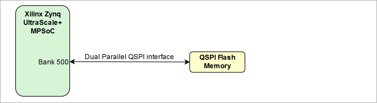
On-board QSPI flash memory U24 and U25 on the TEC0850 board is provided by Micron Serial NOR Flash Memory N25Q256A with 256 Mbit (32 MByte) storage capacity each, 64 MByte total QSPI Flash memory. The QSPI Flash memory ICs are connected to the PS MIO bank (Dual QSPI MIO0 ... MIO12) of the Zynq Ultrascale+ MPSoC, enabling dual parallel booting from QSPI Flash memory. This nonvolatile memory is used to store an initial FPGA configuration. Besides FPGA configuration, remaining free flash memory can be used for user application and data storage. All four SPI data lines are connected to the Zynq MPSoC allowing x1, x2 or x4 data bus widths. Maximum data rate depends on the selected bus width and clock frequency used.
| Scroll Title | ||||||||||||||||||||||||||||||||
|---|---|---|---|---|---|---|---|---|---|---|---|---|---|---|---|---|---|---|---|---|---|---|---|---|---|---|---|---|---|---|---|---|
| ||||||||||||||||||||||||||||||||
|
| Scroll Title | |||||||||||||||||||||||||||||||||||||||||||||||||||||||||||||||
|---|---|---|---|---|---|---|---|---|---|---|---|---|---|---|---|---|---|---|---|---|---|---|---|---|---|---|---|---|---|---|---|---|---|---|---|---|---|---|---|---|---|---|---|---|---|---|---|---|---|---|---|---|---|---|---|---|---|---|---|---|---|---|---|
| |||||||||||||||||||||||||||||||||||||||||||||||||||||||||||||||
|
EEPROMs
The TEC0850 board contains several EEPROMs for configuration and general user purposes. The EEPROMs are provided by Microchip, the I²C interfaces are connected to Zynq MPSoC bank 502 MIO 20...21 pins:
| Scroll Title | ||||
|---|---|---|---|---|
| ||||
|
Quad-SPI Flash Memory
On-board QSPI flash memory U24 and U25 on the TEC0850 board is provided by Micron Serial NOR Flash Memory N25Q256A with 256 Mbit (32 MByte) storage capacity each, 64 MByte total QSPI Flash memory. The QSPI Flash memory ICs are connected to the PS MIO bank (Dual QSPI MIO0 ... MIO12) of the Zynq Ultrascale+ MPSoC, enabling dual parallel booting from QSPI Flash memory. This non volatile memory is used to store initial FPGA configuration. Besides FPGA configuration, remaining free flash memory can be used for user application and data storage. All four SPI data lines are connected to the Zynq MPSoC allowing x1, x2 or x4 data bus widths. Maximum data rate depends on the selected bus width and clock frequency used.
| Scroll Title | |||||||||||||||||||||||||||||
|---|---|---|---|---|---|---|---|---|---|---|---|---|---|---|---|---|---|---|---|---|---|---|---|---|---|---|---|---|---|
| anchor | Figure_11 | title | Figure 11: CAN interface
|
The EEPROMs U63 and U64 are programmable via the onboard I²C bus connected to MIO 20...21 pins. The I²C address is shown in the table below.
| scroll- | ||||||||||||||||||
|---|---|---|---|---|---|---|---|---|---|---|---|---|---|---|---|---|---|---|
| scroll-title | ||||||||||||||||||
| ||||||||||||||||||
| ||||||||||||||||||
| IC | Memory Density | MIO | Signal Schematic Name | Flash Memory Pin | ||||||||||||||
QSPI Flash U24, N25Q256A11E1240E | 256 Mbit (32 MByte) | 0 | MIO0 | B2 | ||||||||||||||
| 1 | MIO1 | D2 | ||||||||||||||||
| 2 | MIO2 | C4 | ||||||||||||||||
| 3 | MIO3 | D4 | ||||||||||||||||
| 4 | MIO4 | D3 | ||||||||||||||||
| 5 | MIO5 | C2 | ||||||||||||||||
QSPI Flash U25, N25Q256A11E1240 | 256 Mbit (32 MByte) | 7 | MIO7 | C2 | ||||||||||||||
| 8 | MIO8 | D3 | ||||||||||||||||
| 9 | MIO9 | D2 | ||||||||||||||||
| 10 | MIO10 | C4 | ||||||||||||||||
| 11 | MIO11 | D4 | ||||||||||||||||
| 12 | MIO12 | B2 |
EEPROMs
|
USB2 PHY
USB2 PHY U11 is provided by USB3320 from Microchip. The ULPI interface is connected to the Zynq Ultrascale+ PS USB0. I/O voltage is fixed at 1.8V and PHY reference clock input is supplied from the on-board 52.000000 MHz oscillator U12. There is also the option to equip the TEC0850 board with a second USB2 PHY U13 connected to the optional cPCI backplane connector J3. Both, the optional USB2 PHY U13 and cPCI connector J3 are not fitted by default.The TEC0850 board contains several EEPROMs for configuration and general user purposes. The EEPROMs are provided by Microchip, the I²C interfaces is connected to Zynq MPSoC bank 502 MIO 20...21 pins:
| Scroll Title | ||||||
|---|---|---|---|---|---|---|
| ||||||
| Scroll Ignore | ||||||
| draw.io Diagram | ||||||
| border | true | |||||
| viewerToolbar | true | |||||
| fitWindow | false | |||||
| diagramName | TEC0850 USB3 to FIFO | |||||
| simpleViewer | false | width | ||||
| diagramWidth | 641 | |||||
| revision | 2 | |||||
| Scroll Only |
The EEPROMs U63 and U64 are programmable via the on-board I²C bus connected to MIO 20...21 pins. The I²C address is shown in the table below.
...
| anchor | Table_x |
|---|---|
| title | Table x: EEPROMs I2C Addresses |
...
| ||||||||||||||||||||||||||||||||
|
| Scroll Title | ||||||||||||||||||||||||||||||||||||||||||||||
|---|---|---|---|---|---|---|---|---|---|---|---|---|---|---|---|---|---|---|---|---|---|---|---|---|---|---|---|---|---|---|---|---|---|---|---|---|---|---|---|---|---|---|---|---|---|---|
| ||||||||||||||||||||||||||||||||||||||||||||||
|
USB2 PHY
USB2 PHY U15 is provided by USB3320 from Microchip. The ULPI interface is connected to the Zynq Ultrascale+ PS USB0. I/O voltage is fixed at 1.8V and PHY reference clock input is supplied from the on-board 52.000000 MHz oscillator U12.
| Scroll Title | ||||
|---|---|---|---|---|
| ||||
| Scroll Ignore | ||||
| draw.io Diagram | ||||
| border | true | |||
| viewerToolbar | true | |||
| fitWindow | false | |||
| diagramName | TEC0850 USB2 PHY | |||
| simpleViewer | false | width | ||
| diagramWidth | 641 | |||
| revision | 1 | |||
| Scroll Only | ||||
| Scroll Title | ||||
| ||||
| Scroll Table Layout | | |||
| orientation | portrait | |||
| sortDirection | ASC | |||
| repeatTableHeaders | default | style | widths | |
| sortByColumn | 1 | |||
| sortEnabled | false | |||
| cellHighlighting | true |
| PHY Pin | Connected to | Notes | |
|---|---|---|---|
| ULPI | PS bank MIO52 MIO64 ... MIO63MIO75 | Zynq Ultrascale+ | USB0USB1 MIO pins are connected to the PHY |
| REFCLK | - | 52MHz from | on boardonboard oscillator U12 |
| REFSEL[0..2] | - | All pins set to GND selects the external reference clock frequency (52.000000 MHz) | |
| RESETB | Zynq MPSoC MIO16MIO17, pin AM16AP16 | Low active USB2 PHY Reset | |
| DP, DM | optional cPCI connector J1J3 | USB2 data lane | |
| CPEN | - | External USB power switch active-high enable signal | |
| VBUS | 5V | Connected to USB VBUS onboard 5V voltage level via a series of resistors, see schematic | |
| ID | 3.3V | B-deviceUSB2 OTG A-Device (host) |
Gigabit Ethernet PHY
On-board Onboard Gigabit Ethernet PHY U20 is provided with Marvell Alaska 88E1512, which use MDIO address 1.. The Ethernet PHY RGMII interface is connected to the Zynq Ultrascale+ Ethernet0 PS GEM3. I/O voltage is fixed at 1.8V for HSTL signaling. The reference clock input of the PHY is supplied from the on-board 25.000000 MHz oscillator U21.
| Scroll Title | |||||||||||||||||||||||||||||||||||||||
|---|---|---|---|---|---|---|---|---|---|---|---|---|---|---|---|---|---|---|---|---|---|---|---|---|---|---|---|---|---|---|---|---|---|---|---|---|---|---|---|
| |||||||||||||||||||||||||||||||||||||||
|
8bit DACs
The TEC0850 Board has 4 8-bit parallel Texas Instruments THS5641AIPW digital to analog converter (DAC) with up to 100 MSPS update rate connected to TI THS4631D operational amplifiers. See Schematic circuitry and TI THS5641 data sheet for proper operation of the on-board DAC units.
| Scroll Title | ||||||||||||||||||||||||||||||||||||||||||||||||||||||||||||||||||||||||||||||||||||||||||||||||||||||||||||||||||||||||||||||||||
|---|---|---|---|---|---|---|---|---|---|---|---|---|---|---|---|---|---|---|---|---|---|---|---|---|---|---|---|---|---|---|---|---|---|---|---|---|---|---|---|---|---|---|---|---|---|---|---|---|---|---|---|---|---|---|---|---|---|---|---|---|---|---|---|---|---|---|---|---|---|---|---|---|---|---|---|---|---|---|---|---|---|---|---|---|---|---|---|---|---|---|---|---|---|---|---|---|---|---|---|---|---|---|---|---|---|---|---|---|---|---|---|---|---|---|---|---|---|---|---|---|---|---|---|---|---|---|---|---|---|---|
| ||||||||||||||||||||||||||||||||||||||||||||||||||||||||||||||||||||||||||||||||||||||||||||||||||||||||||||||||||||||||||||||||||
|
...
There are two 4-bit DIP-witches S3 and S4 present on the TEC0850 board to configure options and set parameters. The following section describes the functionalities of the particular switches.
Table The table below describes the functionalities of the switches of DIP-switches S1 and S2 at their each positionsevery position:
| Scroll Title | ||||||||||||||||||||||||||||||||||||||||||||||||||||||||||||||||||||||||||||||||||||||||||||||||||
|---|---|---|---|---|---|---|---|---|---|---|---|---|---|---|---|---|---|---|---|---|---|---|---|---|---|---|---|---|---|---|---|---|---|---|---|---|---|---|---|---|---|---|---|---|---|---|---|---|---|---|---|---|---|---|---|---|---|---|---|---|---|---|---|---|---|---|---|---|---|---|---|---|---|---|---|---|---|---|---|---|---|---|---|---|---|---|---|---|---|---|---|---|---|---|---|---|---|---|
| ||||||||||||||||||||||||||||||||||||||||||||||||||||||||||||||||||||||||||||||||||||||||||||||||||
|
...
There is one switch button available to the user connected to the SC FPGA U18:
| Scroll Title | |||||||||||||||||||||||||||
|---|---|---|---|---|---|---|---|---|---|---|---|---|---|---|---|---|---|---|---|---|---|---|---|---|---|---|---|
| |||||||||||||||||||||||||||
|
...
The TEC0850 board is equipped with several LEDs to signal current states and activities.
| Scroll Title | ||||||||||||||||||||||||||||||||||||||
|---|---|---|---|---|---|---|---|---|---|---|---|---|---|---|---|---|---|---|---|---|---|---|---|---|---|---|---|---|---|---|---|---|---|---|---|---|---|---|
| ||||||||||||||||||||||||||||||||||||||
|
...
The maximum power consumption of a module mainly depends on the design running on the FPGA.
Xilinx provide provides a power estimator excel sheets to calculate power consumption. It's also possible to evaluate the power consumption of the developed design with Vivado. See also Trenz Electronic Wiki FAQ.
| Scroll Title | ||||||||||||||||||||||
|---|---|---|---|---|---|---|---|---|---|---|---|---|---|---|---|---|---|---|---|---|---|---|
| ||||||||||||||||||||||
|
Power supply with a minimum current capability of 6.65A 5A (60W@12V, CompactPCI Serial spec.) for system startup is recommended.
The TEC0850 board is equipped with the Xilinx Zynq UltraScale+ MPSoC delivers a heterogeneous multi-processing system with integrated programmable logic and independently operable elements and is designed to meet an embedded system power management requirement by advanced power management features. This These features allow to offset offsetting the power and heat constraints against overall performance and operational efficiency.
...
There are following dependencies how the initial 24V voltage from the main power pins on cPCI slot J1 is distributed to the on-board onboard DC-DC converters, which power up further DC-DC converters and the particular on-board voltages:
| Scroll Title | ||||||||||||||||||||||||||||||||||||
|---|---|---|---|---|---|---|---|---|---|---|---|---|---|---|---|---|---|---|---|---|---|---|---|---|---|---|---|---|---|---|---|---|---|---|---|---|
| ||||||||||||||||||||||||||||||||||||
|
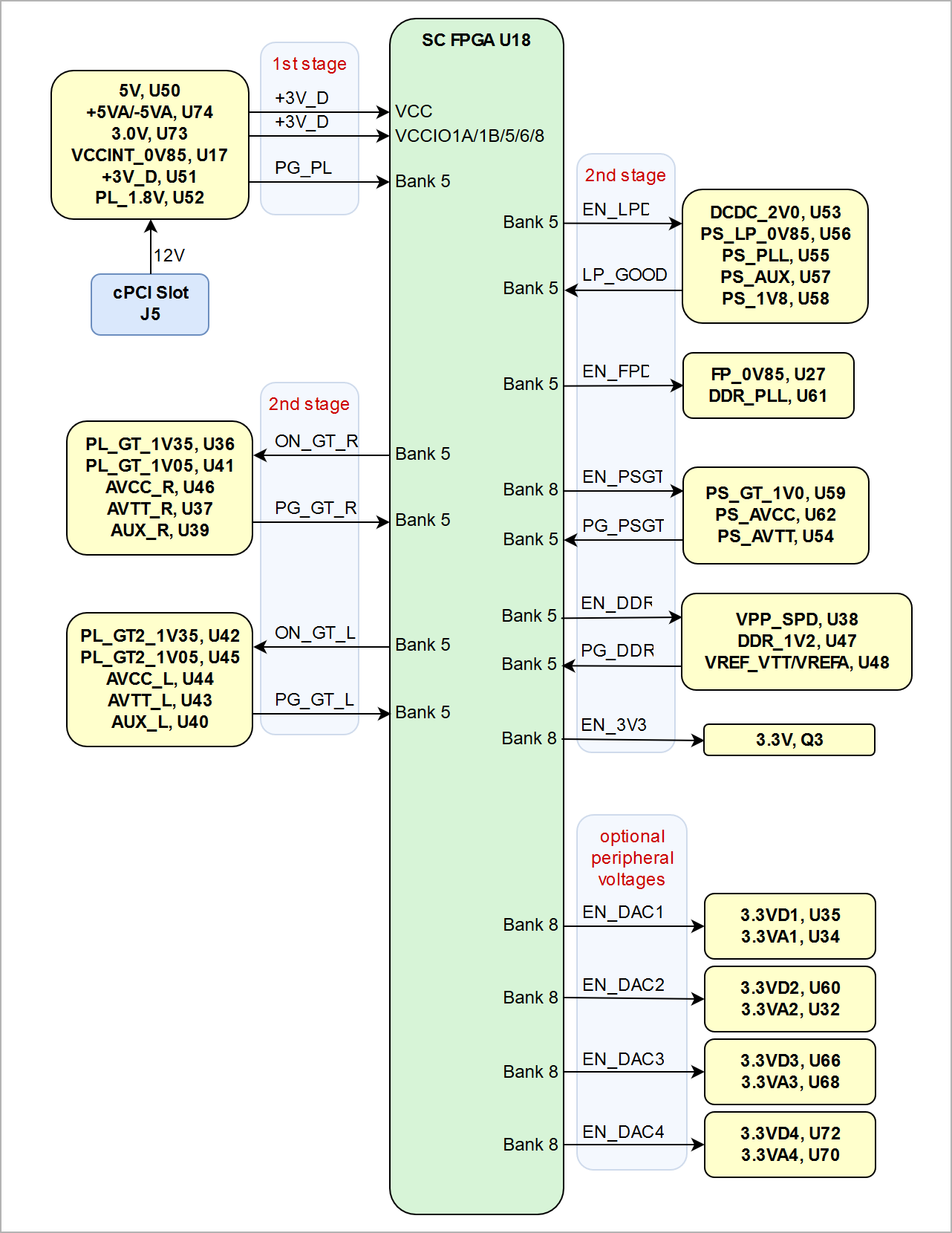
Power-On Sequence
The TEC0850 board meets the recommended criteria to power up the Xilinx Zynq UltraScale+ MPSoC properly by keeping a specific sequence of enabling the on-board onboard DC-DC converters dedicated to the particular Power Domains and powering up the on-board onboard voltages.
On the TEB0911 UltraRack board following Power Domains will be powered up in a certain sequence with by enable and power-good signals of the DC-DC converters, which are controlled by the System Controller FPGA U18:
...
Hence, those three power instances will be powered up consecutively when the Power-Good signals of the previous instance is are asserted.
Following diagram describes the sequence of enabling the three power instances utilizing the DC-DC converter control signals (Enable, Power-Good), which will power-up in descending order as listed in the blocks of the diagram.
| Scroll Title | ||||||||||||||||||||||||||||||||||
|---|---|---|---|---|---|---|---|---|---|---|---|---|---|---|---|---|---|---|---|---|---|---|---|---|---|---|---|---|---|---|---|---|---|---|
| ||||||||||||||||||||||||||||||||||
|
| Warning |
|---|
| To avoid any damage to the MPSoC module, check for stabilized on-board voltages in steady onboard voltages in a steady state before powering up the MPSoC's I/O bank voltages VCCOx. All I/Os should be tri-stated during the power-on sequence. |
It is important that all PS and PL I/Os are tri-stated at power-on until the "Power Good"-signals are high, meaning that all on-board onboard voltages have become stable and the module is properly powered up.
...
| Scroll Title | ||||||||||||||||||||||||||||||||||||
|---|---|---|---|---|---|---|---|---|---|---|---|---|---|---|---|---|---|---|---|---|---|---|---|---|---|---|---|---|---|---|---|---|---|---|---|---|
| ||||||||||||||||||||||||||||||||||||
|

Power Rails
| Scroll Title | ||||||||||||||||||||||||||||||||||||||||||||||||||||||||||||||||||||||||||
|---|---|---|---|---|---|---|---|---|---|---|---|---|---|---|---|---|---|---|---|---|---|---|---|---|---|---|---|---|---|---|---|---|---|---|---|---|---|---|---|---|---|---|---|---|---|---|---|---|---|---|---|---|---|---|---|---|---|---|---|---|---|---|---|---|---|---|---|---|---|---|---|---|---|---|
| ||||||||||||||||||||||||||||||||||||||||||||||||||||||||||||||||||||||||||
|
Bank Voltages
| Scroll Title | |||||||||||||||||||||||||||||||||||||||||||||||||||||||||||||||||||||||||||||||||||||||||||||||||||||||||||||||||||||||||||||||||||||||||||||||
|---|---|---|---|---|---|---|---|---|---|---|---|---|---|---|---|---|---|---|---|---|---|---|---|---|---|---|---|---|---|---|---|---|---|---|---|---|---|---|---|---|---|---|---|---|---|---|---|---|---|---|---|---|---|---|---|---|---|---|---|---|---|---|---|---|---|---|---|---|---|---|---|---|---|---|---|---|---|---|---|---|---|---|---|---|---|---|---|---|---|---|---|---|---|---|---|---|---|---|---|---|---|---|---|---|---|---|---|---|---|---|---|---|---|---|---|---|---|---|---|---|---|---|---|---|---|---|---|---|---|---|---|---|---|---|---|---|---|---|---|---|---|---|---|
| |||||||||||||||||||||||||||||||||||||||||||||||||||||||||||||||||||||||||||||||||||||||||||||||||||||||||||||||||||||||||||||||||||||||||||||||
|
...
Absolute Maximum Ratings
| Scroll Title | ||||||||||||||||||||||||||||||||||||||||||||||||||||||||||||||||||||||||||||||||||||||||||||||||||||||||||||
|---|---|---|---|---|---|---|---|---|---|---|---|---|---|---|---|---|---|---|---|---|---|---|---|---|---|---|---|---|---|---|---|---|---|---|---|---|---|---|---|---|---|---|---|---|---|---|---|---|---|---|---|---|---|---|---|---|---|---|---|---|---|---|---|---|---|---|---|---|---|---|---|---|---|---|---|---|---|---|---|---|---|---|---|---|---|---|---|---|---|---|---|---|---|---|---|---|---|---|---|---|---|---|---|---|---|---|---|---|
| ||||||||||||||||||||||||||||||||||||||||||||||||||||||||||||||||||||||||||||||||||||||||||||||||||||||||||||
|
Recommended Operating Conditions
| Scroll Title | ||||||||||||||||||||||||||||||||||||||||||||||||||||||||||||||||||||||||||||||
|---|---|---|---|---|---|---|---|---|---|---|---|---|---|---|---|---|---|---|---|---|---|---|---|---|---|---|---|---|---|---|---|---|---|---|---|---|---|---|---|---|---|---|---|---|---|---|---|---|---|---|---|---|---|---|---|---|---|---|---|---|---|---|---|---|---|---|---|---|---|---|---|---|---|---|---|---|---|---|
| ||||||||||||||||||||||||||||||||||||||||||||||||||||||||||||||||||||||||||||||
|
1) Temperature range may vary depending on assembly options
2) The operating temperature range of the Zynq MPSoC, SC FPGA SoC and on-board onboard peripherals are a junction and also ambient operating temperature ranges
...
| Scroll Title | ||||
|---|---|---|---|---|
| ||||
|
...
| Page properties | ||||
|---|---|---|---|---|
| ||||
|
| Scroll Title | ||||||||||||||||||||||
|---|---|---|---|---|---|---|---|---|---|---|---|---|---|---|---|---|---|---|---|---|---|---|
| ||||||||||||||||||||||
| ||||||||||||||||||||||
...
Hardware Revision History
| Scroll Title | |||||||||||||||||||||||||||||||||||
|---|---|---|---|---|---|---|---|---|---|---|---|---|---|---|---|---|---|---|---|---|---|---|---|---|---|---|---|---|---|---|---|---|---|---|---|
| |||||||||||||||||||||||||||||||||||
Notes
current available board revision
|
Document Change History
| Page properties | ||||
|---|---|---|---|---|
| ||||
|
| Scroll Title | ||||||||||||||||||||||||||||||||||||||||||||||||||||||||||||||||||||||||||||||||||||||||||||
|---|---|---|---|---|---|---|---|---|---|---|---|---|---|---|---|---|---|---|---|---|---|---|---|---|---|---|---|---|---|---|---|---|---|---|---|---|---|---|---|---|---|---|---|---|---|---|---|---|---|---|---|---|---|---|---|---|---|---|---|---|---|---|---|---|---|---|---|---|---|---|---|---|---|---|---|---|---|---|---|---|---|---|---|---|---|---|---|---|---|---|---|---|
| ||||||||||||||||||||||||||||||||||||||||||||||||||||||||||||||||||||||||||||||||||||||||||||
|
Disclaimer
| Include Page | ||||
|---|---|---|---|---|
|
...
Overview
Content Tools