Download PDF version of this document.
Table of Contents
Overview
The Trenz Electronic TEC0850 board is a CompactPCI card (3U form factor) integrating a Xilinx Zynq UltraScale+ MPSoC, one DDR4 SDRAM SODIMM socket with 64bit wide databus, max. dual 512 MByte Flash memory for configuration and operation, 24 Gigabit transceivers on PL side and 4 on PS side, powerful switch-mode power supplies for all on-board voltages, USB2 and USB3 FIFO bridges and a large number of configurable I/Os available on the CompactPCI backplane connectors.
Refer to http://trenz.org/tec0850-info for the current online version of this manual and other available documentation.
Key Features
Zynq UltraScale+ MPSoC ZU15
- Front side interface connectors
- RJ-45 GbE Ethernet interface
- Circular push/pull connector with 4x on-board 8bit DAC output
- MicroSD Card connector
- USB2 and USB3 to FIFO bridge connector
- 4x status LEDs
- 4 CompactPCI connectors for backplane connection (3U form factor)
- 24 GTH lanes
- 4 PS GTR lanes
- USB2 interface
- 64 Zynq PL HP I/O's
- 8x PLL clock input
- JTAG, I²C and 7 user I/O's to MAX10 FPGA
64bit DDR4 SODIMM (PS connected), 8 GByte maximum
Dual parallel QSPI Flash (bootable), 512 MByte maximum
- 26-pin header with 20 Zynq PL HD I/O's
- 3-pin header with 2 MAX10 FPGA I/O's
- System Controller (Altera MAX10 FPGA SoC)
- Power Sequencing
- System management and control for MPSoC and on-board peripherals
- Si5345 programmable 10 output PLL clock generator
- Si53340 Quad clock buffer
- 2x 4bit DIP switches
- 1x user push button
- Zynq MPSoC cooling FAN connector
- On-board high-efficiency DC-DC converters
Block Diagram
Figure 1: TEC0850-02 block diagram
Main Components
Figure 2: TEC0850-02 main components
- GbE RJ-45 MagJack, J7
- 5-pin circular push/pull receptacle connector for DAC output, J15
- Micro USB2 B receptacle connector, J9
- MicroSD Card socket, J11
- USB C connector, J10
- LED light pipes J14 integrating LEDs D1 ... D4
- 4bit DIP-switch, S2
- 4bit DIP-switch, S1
- FTDI FT2232 USB2 to FIFO bridge, U4
- 3-pin PicoBlade header, J8
- MAX10 FPGA JTAG/UART 10-pin header, J13
- Altera MAX10 System Controller FPGA, U18
- 4-Wire PWM fan connector, J17
- 26-pin IDC header for FPGA PL I/O's, J16
- DDR4 SO-DIMM 260-pin socket, U3
- Battery Holder CR1220, B1
- 256 Mbit (32 MByte) Micron Serial NOR Flash Memory N25Q256A, U24
- 256 Mbit (32 MByte) Micron Serial NOR Flash Memory N25Q256A, U25
- DC-DC Converter LT8471IFE @+5VA/-5VA, U74
- DC-DC Converter EM2130L02QI @VCCINT_0V85, U17
- DC-DC Converter 171050601 @5V, U50
- Xilinx Zynq Ultrascale+ MPSoC, U1
- Si5345A 10-output I²C programmable PLL clock, U14
- Main power fuse @2.5A/16V, F1
- cPCI connector, J1
- cPCI connector, J4
- cPCI connector, J5
- cPCI connector, J6
- FTDI FT601Q USB3 to FIFO bridge, U9
- TI THS5641 8bit DAC ,U28
- TI THS5641 8bit DAC ,U31
- TI THS5641 8bit DAC ,U29
- TI THS5641 8bit DAC ,U33
- Marvell Alaska 88E1512 GbE PHY ,U20
Initial Delivery State
Storage device name | Content | Notes |
|---|---|---|
| User configuration EEPROMs (1x Microchip 24AA128T-I/ST, 1x Microchip 24AA025E48T-I/OT) | Empty | Not programmed |
| USB2 to FIFO bridge configuration EEPROM (ST M93C66) | Empty | Not programmed |
| Si5345A programmable PLL NVM OTP | Empty | Not programmed |
| 2x QSPI Flash memory | Empty | Not programmed |
Table 1: Initial delivery state of programmable devices on the module.
Control Signals
Signals, Interfaces and Pins
CompactPCI Backplane Connectors
The TEC0850 board is equipped with 3 CompactPCI high speed backplane connectors which provides serial high-speed interconnects with transmission rates up to 12 Gb/s to the Zynq MPSoCs MGT lanes, high speed USB2 interface and single ended FPGA I/O pins Zynq MPSoC and the System Controller FPGA.
The connectors support single ended and differential signaling as the Zynq MPSoC FPGA I/O's are routed from the FPGA banks as LVDS-pairs to the backplane connector.
The TEC0850 board is designed to be connected to the System Slot of the backplane connector, whereby 4 of the 6 connectors of the System Slot configuration are fitted to the TEC0850 board.
Following diagram gives an overview of the CompactPCI backplane connectors and their connections to the Zynq Ultrascale+ MPSoC and the System Controller FPGA U18:
Figure 3: TEC0850-02 CompactPCI I/O and high-speed interfaces
Following tables contains information about the interfaces, I/O's, clock and VCCIO sources available on the cPCI connectors:
CompactPCI Connector J1
| Interfaces | I/O Signal Count | LVDS-pairs count | Connected to | VCCO bank Voltage | Notes |
|---|---|---|---|---|---|
| I/O | 1 | - | SC FPGA U18 Bank 6 | +3V_D | control signals in cPCI pin assingment |
| 6 | - | SC FPGA U18 Bank 8 | +3V_D | control signals in cPCI pin assingment | |
| I²C | 2 | - | SC FPGA U18 Bank 1A | +3V_D | SC FPGA U18 I²C interface |
| JTAG | 4 | - | SC FPGA U18 Bank 1A | +3V_D | SC FPGA U18 JTAG interface |
| MGT | - | 8 (4 x RX/TX) | Bank 502 PS GTR | - | 4x PS GTR lanes |
| USB2 | - | 1 (RX/TX) | USB2 PHY U11 | - | USB2 OTG A-Device (host) |
| Clock Input | - | 1 | Clock Driver U73 | - | 1x Reference clock input from PLL clock U14 |
Table 2: cPCI J1 interfaces
| MGT Lane | Bank | Type | Signal Schematic Name | cPCI Connector Pin | FPGA Pin |
|---|---|---|---|---|---|
| 0 | 505 | GTR |
| J1-D5 | PS_MGTRRXP0_505, AB29 |
| 1 | 505 | GTR |
| J1-J5 | PS_MGTRRXP1_505, Y29 |
| 2 | 505 | GTR |
| J1-E6 | PS_MGTRRXP2_505, W31 |
| 3 | 505 | GTR |
| J1-K6 | PS_MGTRRXP3_505, V29 |
Table 3: cPCI J1 MGT lanes
| Clock Signal Schematic Name | cPCI Connector Pin | Header J13 Pin | SC FPGA U18 Pin | Notes |
|---|---|---|---|---|
| J1-K3 | J13-5 | Bank 1B, Pin G1 | Supplied by 10-output PLL clock U14, cPCI connector J1 clock signal from PLL U14 is |
Table 4: cPCI J1 clock signals
| Available VCC/VCCIO | cPCI Connector Pin | Source | Notes |
|---|---|---|---|
| VIN_12V | J1-A1 | cPCI backplane | min. cur.: 6.65A |
Table 5: cPCI J1 VCC/VCCIO
CompactPCI Connector J4
| MGT Lane | Bank | Type | Signal Schematic Name | cPCI Connector Pin | FPGA Pin |
|---|---|---|---|---|---|
| 0 | 128 | GTH |
| J4-D1 | MGTHRXP0_128, T33 |
| 1 | 128 | GTH |
| J4-J1 | MGTHRXP1_128, P33 |
| 2 | 128 | GTH |
| J4-E2 | MGTHRXP2_128, N31 |
| 3 | 128 | GTH |
| J4-K2 | MGTHRXP3_128, M33 |
| 0 | 129 | GTH |
| J4-D3 | MGTHRXP0_129, L31 |
| 1 | 129 | GTH |
| J4-J3 | MGTHRXP1_129, K33 |
| 2 | 129 | GTH |
| J4-E4 | MGTHRXP2_129, H33 |
| 3 | 129 | GTH |
| J4-K4 | MGTHRXP3_129, F33 |
| 0 | 130 | GTH |
| J4-D5 | MGTHRXP3_130, B33 |
| 1 | 130 | GTH |
| J4-J5 | MGTHRXP2_130, C31 |
| 2 | 130 | GTH |
| J4-E6 | MGTHRXP1_130, D33 |
| 3 | 130 | GTH |
| J4-K6 | MGTHRXP0_130, E31 |
| 0 | 230 | GTH |
| J4-D7 | MGTHRXP3_230, A4 |
| 1 | 230 | GTH |
| J4-J7 | MGTHRXP2_230, B2 |
| 2 | 230 | GTH |
| J4-E8 | MGTHRXP1_230, C4 |
| 3 | 230 | GTH |
| J4-K8 | MGTHRXP0_230, D2 |
Table 6: cPCI J4 MGT lanes
CompactPCI Connector J5
| MGT Lane | Bank | Type | Signal Schematic Name | cPCI Connector Pin | FPGA Pin |
|---|---|---|---|---|---|
| 0 | 228 | GTH |
| J5-D3 | MGTHRXP0_228, T2 |
| 1 | 228 | GTH |
| J5-J3 | MGTHRXP1_228, P2 |
| 2 | 228 | GTH |
| J5-E4 | MGTHRXP2_228, M2 |
| 3 | 228 | GTH |
| J5-K4 | MGTHRXP3_228, L4 |
| 0 | 229 | GTH |
| J5-D1 | MGTHRXP0_229, K2 |
| 1 | 229 | GTH |
| J5-J1 | MGTHRXP1_229, J4 |
| 2 | 229 | GTH |
| J5-E2 | MGTHRXP2_229, H2 |
| 3 | 229 | GTH |
| J5-K2 | MGTHRXP3_229, F2 |
Table 7: cPCI J5 MGT lanes
| PLL Clock U14 Output | Signal Schematic Name | cPCI Connector J5 Pin | Notes |
|---|---|---|---|
| OUT1 |
| J5-A5 | reference clock signals supplied |
| OUT2 |
| J5-D5 | |
| OUT3 |
| J5-G5 | |
| OUT4 |
| J5-J5 | |
| OUT5 |
| J5-B6 | |
| OUT6 |
| J5-E6 | |
| OUT7 |
| J5-H6 | |
| OUT8 |
| J5-K6 |
Table 8: cPCI J5 clock signals
CompactPCI Connector J6
| Interfaces | I/O Signal Count | LVDS-pairs count | Connected to | VCCO bank Voltage | Notes |
|---|---|---|---|---|---|
| I/O | 46 | 23 | PL bank 66 | PL_1.8V | - |
| 18 | 9 | PL bank 65 | PL_1.8V | - | |
| 2 | - | SC FPGA U18 Bank 1B | +3V_D | Signalname: 'DET_RIO', 'DET_BPR' |
Table 9: cPCI J6 Interfaces
USB-C Connector
Front panel USB-C Interface is connected to USB FIFO bridge chip FT601Q. 32-bit FIFO bridge provides a simple high-speed interface to Zynq UltraScale+ PL.
Figure 4: TEC0850-02 USB3 to FIFO bridge
The USB3 to FIFO bridge FTDI FT601Q U9 is connected to the Zynq MPSoC's PL bank 64 and is accessible through USB-C connector J10:
| Interface | Signal Schematic Names | Connected to | Notes |
|---|---|---|---|
| USB3 data lane |
| USB C Connector J10 | - |
| USB2 data lane |
| USB C Connector J10 | - |
| Control Lines |
| PL bank 64 | - |
| Parallel GPIO's |
| PL bank 64 | 32bit FIFO register |
Table 10: USB-C connector J10
See FT600Q-FT601Q IC Datasheet for interface details.
Micro-USB2 Connector
Front panel Micro-USB2 Interface provides access to UART and JTAG functions via FTDI FT2232 chip. Use of this feature requires that USB driver is installed on your host PC. UART0 with MIO 22 .. 23 should be selected in "Zynq UltraScale+ MPSoC" configuration.
The Digilent plug-in software and cable drivers must be installed on your machine for you to be able to use JTAG interface.
Figure 5: JTAG/UART Interface
The USB2 to FIFO bridge FTDI FT2232H U4 is connected to the SC FPGA U18 and is accessible through Micro-USB2 connector J9:
| Interface | Signal Schematic Names | Connected to | Notes |
|---|---|---|---|
| USB2 data lane |
| Micro-USB2 connector J9 | - |
| Control Lines |
| SC FPGA U18, bank 6 | - |
| Parallel GPIO's |
| SC FPGA U18, bank 6 | - |
Table 11: Micro-USB2 connector J9
SD
The SD Card interface of the TEC0850 board is not directly wired to the connector J11 pins, but through a Texas Instruments TXS02612 SD IO Port Expander, which is needed for voltage translation due to different voltage levels of the Micro SD Card and MIO-bank of the Xilinx Zynq MPSoC. The Micro SD Card has 3.3V signal voltage level, but the PS MIO-bank on the Xilinx Zynq MPSoC has VCCIO of 1.8V.
Figure 6: MicroSD Card interface
There are some limitations to use SD card Interface in Linux.
- Zynq UltraScale+ SD controller is working only in the 3.3V mode as it connected to SD card socket using SD IO port expander U10 as 1.8V to 3.3V level shifter.
- Micro SD card socket has no "Write Protect" switch.
To force Linux driver not to use this features add following instructions to device tree file.
&sdhci1 {
no-1-8-v;
disable-wp;
};
RJ45 - Ethernet
On-board Gigabit Ethernet PHY is provided with Marvell Alaska 88E1512 IC U20. The Ethernet PHY RGMII interface is connected to the Zynq MPSoC Ethernet interface of the PS MIO bank 501. I/O voltage is fixed at 1.8V for HSTL signaling. The reference clock input of the PHY is supplied from the on-board 25.000000 MHz oscillator U21. The LEDs of the RJ-45 MegJack J13 are connected to the GbE PHY U20 status LED output.
Figure 7: Gigabit Ethernet Interface
DDR4 SODIMM Socket
On the TEC0850 board there is a DDR4 memory interface U3 with a 64-bit databus width available for SO-DIMM modules connected to the Zynq UltraScale+ DDRC hard memory controller.
Figure 8: DDR4 SDRAM SODIMM socket
Following table gives an overview about the memory interface I/O signals of the DDR4 SDRAM SO-DIMM Socket U3:
| DDR4 SDRAM I/O Signal | Signal Schematic Name | Connected to | Notes |
|---|---|---|---|
| Address inputs |
| PS DDR Bank 504 | - |
| Bank address inputs |
| - | |
| Bank group inputs |
| - | |
| Differential clocks |
| 2 x DDR4 clock | |
| Data input/output |
| - | |
| Check bit input/output |
| - | |
| Data strobe (differential) |
| - | |
| Data mask and data bus inversion |
| - | |
| Serial address inputs |
| address range configuration on I²C bus | |
| Control Signals |
| chip selest signal | |
| On-die termination enable | ||
| nRESET | ||
| Command and address parity input | ||
| Clock enable | ||
| CRC error flag | ||
| Activation command input | ||
| Temperature event | ||
| I²C |
| not connected | - |
Table 12: DDR4 SDRAM SO-DIMM socket U3
Circular Push Pull Connector
The TEC0850 board provides 4x DAC analog voltage output on the 5-pin circular push/pull connector J15. Each of the DAC units consists of one Texas Instruments THS5641AIPW digital to analog converter, TI THS4631D operational amplifier and two LDOs, by which the DAC unit can be switched on and off.
The TI THS4631D digital to analog converter wired to the operational amplifier circuitry creating the DAC unit with a voltage output range from -0.5V ... 0.5V. See TI THS5641 datasheet and schematic how to control the DAC unit and to set the analog output voltages on connector J15.
Figure 9: 4x 8bit DAC units
26-Pin IDC Header
There is a 26-pin IDC header (2x13, 1.27mm grid size) J16 available on the TEC0850 board which exposes the 20 FPGA HD I/O's of PL bank 47 to the user. The PL bank 47 has 3.3V VCCO bank voltage, on the header J16 there also the voltage levels 3.3V and 5V available. The I/O's can be accessed with a corresponding IDC connector.
Figure 10: Zynq MPSoC PL I/O's IDC pin-header
10-Pin Header
On the TEC0850 there is a 10-pin SMT header (2x5, 2.54mm grid size) J13 present which provides access to the JTAG and UART interface of Altera MAX10 System Controller FPGA. The header J13 has a compatible pin assignment to the TEI0004 JTAG programmer for Altera FPGAs, the voltage levels 3.3V is on the header available as reference I/O-voltage for JTAG and UART.
The 4 JTAG pins of the header J13 are also connected to the cPCI connector J1 and can be used es user GPIO's of the SC FPGA U18 with othr functionalities then JTAG.
On the header J13 there is also a reference clock signal from PLL clcok U14 available, which can be also used for the SC FPGA U18 and on the cPCI connector J1.
Figure 11: 10-pin JTAG/UART header
3-Pin PicoBlade Header
2 I/O's of the SC FPGA U18 are exposed to the on-board 3-Pin PicoBlade header J8 available to the user or for future use of upcoming versions of SC FPGA firmware.
Figure 12: 3-pin PicoBlade header
Battery Holder
There is a CR1220 battery holder available to the supply the voltage for the for for the Zynq MPSoC's Battery Power Domain (BBRAM and RTC). The battery voltage VBATT should be in the range of 2.2V to 5.5V, use 3.0V CR1220 battery.
Figure 13: Backup-Battery Holder
4-Wire PWM FAN Connectors
The TEC0850 offers one 4-wire PWM FAN connector FPGA cooling fan controlled by SC FPGA U18:
Figure 14: 4-wire PWM FAN connector
On-board Peripherals
Zynq UltraScale XCZU15EG MPSoC
The TEC0850 board is populated with the Zynq UltraScale+ XCZU15EG-1FFVB1156E MPSoC.
The PS MIO pins are routed to the on-board peripherals as follows:
| PS MIO | Function | Connected to |
|---|---|---|
| 0 | SPI0 | U24-B2, CLK |
| 1 | SPI0 | U24-D2, DO/IO1 |
| 2 | SPI0 | U24-C4, WP/IO2 |
| 3 | SPI0 | U24-D4, HOLD/IO3 |
| 4 | SPI0 | U24-D3, DI/IO0 |
| 5 | SPI0 | U24-C2, CS |
| 6 | - | Not connected |
| 7 | SPI1 | U25-C2, CS |
| 8 | SPI1 | U25-D3, DI/IO0 |
| 9 | SPI1 | U25-D2, DO/IO1 |
| 10 | SPI1 | U17-C4, WP/IO2 |
| 11 | SPI1 | U25-D4, HOLD/IO3 |
| 12 | SPI1 | U25-B2, CLK |
| 13 ... 15 | - | not connected |
| 16 | USB2 PHY Reset | USB2 PHY U11 |
| 17 | - | not used |
| 18 ... 19 | - | not connected |
| 20 ...21 | PS MIO I²C | I²C peripherals |
| 22 ... 25 | user MIO | SC FPGA U18, bank 2 |
| 26 ... 38 | RGMII | GbE PHY U20 |
| 39 ... 44 | - | not connected |
| 45 ... 51 | SD IO | MicroSD Card socket J11 |
| 52 ... 63 | USB2 ULPI | USB2 PHY U11 |
| 64 ... 75 | - | not used |
| 76 ... 77 | ETH MDC / MDIO | GbE PHY U20 |
Table 13: Default MIO Configuration
MAX10 System Controller FPGA
The TEC0850 board is equipped with one System Controller FPGA (Intel MAX10 10M08SAU169C8G) with the schematic designators U18. The SC FPGA is the central system management unit where essential control signals are logically linked by the implemented logic in FPGA firmware, which generates output signals to control the system, the on-board peripherals and the interfaces. Interfaces like JTAG and UART between the FTDI FT2232H chip and to the Zynq MPSoC are by-passed, forwarded and controlled by the System Controller FPGA.
Other tasks of the System Controller FPGA are the monitoring of the power-on sequence and to display the programming state of the FPGA module. The functionalities and configuration of the pins depend on the SC FPGA's firmware. The documentation of the firmware of SC FPGA U18 contains detailed information on this matter.
The Sytem Controller FPGA is connected to the Zynq Ultrascale+ MPSoC through MIO and PL pins. The signals of these pins are forwarded by the SC FPGA to control some of the on board peripherals.
Following block diagram visualizes the connection of the SC FPGA with the Zynq Ultrascale+ MPSoC via 4 PS MIO pins (MIO22 ... 25), PS Config control signals and 10 singled ended PL HD bank 48 I/O pins (MAX_IO1 ... MAX_IO10):
Figure 15: TEC0850 MAX10 System Controller FPGA
Programmable Clock Generator
There is a Si5345A U14, Silicon Labs I2C programmable 10-output PLL clock generator on-board to generate various reference clocks for the Zynq MPSoC MGT banks and on-board peripherals.
Figure 16: 10-output I²C programmable clock generator
Following table shows on-board Silicon Labs I2C programmable Si5345A U17 10-output programmable PLL reference clock generator inputs and outputs:
| Si5345A U14 Pin | Signal Schematic Name | Connected to | Clock Direction | Note |
|---|---|---|---|---|
| IN0 |
| 40.000 MHz Oscillator U75 | Input | external reference clock input |
| GND | |||
| IN1 | - | not connected | Input | not used |
| - | not connected | |||
| IN2 | - | not connected | Input | not used |
| - | not connected | |||
| IN3 | - | not connected | Input | not used |
| - | not connected | |||
| OUT0 |
| Quad clock buffer Si53340 U16 | Output | reference clock input to |
| ||||
| OUT1 |
| cPCI J5, pin B5 | Output | reference clock output |
| cPCI J5, pin A5 | |||
| OUT2 |
| cPCI J5, pin C6 | Output | |
| cPCI J5, pin B6 | |||
| OUT3 |
| cPCI J5, pin E5 | Output | |
| cPCI J5, pin D5 | |||
| OUT4 |
| cPCI J5, pin H5 | Output | |
| cPCI J5, pin G5 | |||
| OUT5 |
| cPCI J5, pin K5 | Output | |
| cPCI J5, pin J5 | |||
| OUT6 |
| cPCI J5, pin F6 | Output | |
| cPCI J5, pin E6 | |||
| OUT7 |
| cPCI J5, pin L6 | Output | |
| cPCI J5, pin K6 | |||
| OUT8 |
| cPCI J5, pin I6 | Output | |
| cPCI J5, pin H6 | |||
| OUT9 |
| Clock Driver LTC6975 U73 | Output | reference clock input to |
| ||||
| XA/XB |
| 54.000 MHz quartz oscillator Y3 | Input | Differential quartz oscillator clock input |
| ||||
SCLK, |
|
| BiDir | I²C address 0x69 |
Table 14: SI5345 Clock Outputs
The clock outputs OUT1 and OUT9 are distributed via clock buffer U16 and clock driver U14 to several PL and MGT banks:
| Si53340 U16 Pin | Signal Schematic Name | Connected to | Clock Direction | Note |
|---|---|---|---|---|
| Q0 |
| U1, pin G8 | Output | GTH bank 229 reference clock input |
| Q1 |
| U1, pin Y8 | Output | PL HP bank 66 reference clock input |
| Q2 |
| U1, pin U27 | Output | PS GTR Bank 505 reference clock input |
| Q3 |
| U1, pin L27 | Output | GTH bank 129 reference clock input |
| LTC6957 U14 Pin | ||||
| OUT1 |
| U1, pin AG5 | Output | PL HP bank 65 reference clock input |
| OUT2 |
| Signal 'SATA_SL' | Output | reference clock input cPCI connector J1, header J13 and SC FPGA U18 |
Table 15: Clock driver and buffer outputs
The clock generator U14 is programmable via the on-board I²C bus connected to MIO 20...21 pins. The I²C address is shown in the table below.
| I2C address | Chip | Description |
|---|---|---|
| 0x69 | U14 Si5345 | Clock generator and distributor |
Table 16: SI5345 I2C address
Oscillators
The TEC0850 board is equipped several on-board oscillators to provide the Zynq Ultrascale+ MPSoC's PS and PL banks and the on-board peripherals with reference clock-signals:
| Clock Source | Signal Schematic Name | Frequency | Clock Input Destination |
|---|---|---|---|
| SiTime SiT8008BI oscillator, U22 |
| 33.333333 MHz | Zynq MPSoC U1 PS Config Bank 503, pin U24 |
| SiTime SiT8008AI oscillator, U12 |
| 52.000000 MHz | USB2 transceiver PHY U11, pin 26 |
| SiTime SiT8008AI oscillator, U16 |
| 12.000000 MHz | FTDI FT2232H U4, pin 3 |
| Kyocera CX3225SB30000, Y1 | - | 30.000 MHz | FTDI FT601Q U9, pin 21/22 |
| CM-2012-2pad, Y2 | - | 32.768000 kHz | Zynq MPSoC U1 PS Config Bank 503, pin V21/V22 |
| Kyocera CX3225SB26000, Y3 |
| 54.000 MHz | 10-output PLL clock generator U14, pin 8/9 |
| SiTime SiT8008BI oscillator, U21 |
| 25.000000 MHz | Gigabit Ethernet PHY U20, pin 34 |
| ASVTX-12-A oscillator, U75 |
| 40.000 MHz | 10-output PLL clock generator U14, pin 63 |
Table 17: TEC0850 on-board oscillators
FTDIs
The TEC0850 board is equipped with 2 FTDI chips FT2232H (U4) and FT601Q (U9). Both chips are USB to Multipurpose UART/FIFO bridges which converts signals from USB2 or USB3 to a variety of standard serial and parallel interfaces.
Figure 17: TEC0850 on-board FTDI chips
FT2232H
The TEC0850 board is equipped with the FTDI FT2232H USB2 to JTAG/UART adapter controller connected to micro-USB2 connector J9 to provide JTAG and UART access to the Xilinx Zynq XC7Z010 SoC. There is also a 256-byte configuration EEPROM U6 wired to the FT2232H chip via Microwire bus which holds pre-programmed license code to support Xilinx programming tools. Refer to the FTDI data sheet to get information about the capacity of the FT2232H chip.
Do not access the FT2232H EEPROM using FTDI programming tools, doing so will erase normally invisible user EEPROM content and invalidate stored Xilinx JTAG license. Without this license the on-board JTAG will not be accessible any more with any Xilinx tools. Software tools from FTDI website do not warn or ask for confirmation before erasing user EEPROM content.
Channel A of the FTDI IC is configured as JTAG interface (MPSSE) connected to the SC FPGA U18, the JTAG signals are forwarded to the JTAG interface of the Zynq MPSoC on PS config bank 503.
Channel B can be used as UART Interface routed to SC FPGA U18, 11 I/O's of Channel B are routed to are usable for example as GPIOs and other standard interfaces.
| FT2232H U3 Pin | Signal Schematic Name | Connected to | Notes |
|---|---|---|---|
| Pin 12, ADBUS0 | ADBUS0 | SC FPGA U18 bank 6, pin G9 | JTAG interface |
| Pin 13, ADBUS1 | ADBUS1 | SC FPGA U18 bank 6, pin F10 | |
| Pin 14, ADBUS2 | ADBUS2 | SC FPGA U18 bank 6, pin E10 | |
| Pin 15, ADBUS3 | ADBUS3 | SC FPGA U18 bank 6, pin D9 | |
| Pin 32, BDBUS0 | BDBUS0 | SC FPGA U18 bank 6, pin B11 | UART and |
| Pin 33, BDBUS1 | BDBUS1 | SC FPGA U18 bank 6, pin A12 | |
| Pin 34, BDBUS2 | BDBUS2 | SC FPGA U18 bank 6, pin B12 | |
| Pin 35, BDBUS3 | BDBUS3 | SC FPGA U18 bank 6, pin C11 | |
| Pin 37, BDBUS4 | BDBUS4 | SC FPGA U18 bank 6, pin B13 | |
| Pin 38, BDBUS5 | BDBUS5 | SC FPGA U18 bank 6, pin C12 | |
| Pin 39, BDBUS6 | BDBUS6 | SC FPGA U18 bank 6, pin C13 | |
| Pin 40, BDBUS7 | BDBUS7 | SC FPGA U18 bank 6, pin D11 | |
| Pin 42, BCBUS0 | BCBUS0 | SC FPGA U18 bank 6, pin D12 | |
| Pin 46, BCBUS1 | BCBUS1 | SC FPGA U18 bank 6, pin E13 | |
| Pin 47, BCBUS2 | BCBUS2 | SC FPGA U18 bank 6, pin E12 | |
| Pin 48, BCBUS3 | BCBUS3 | SC FPGA U18 bank 6, pin F13 | |
| Pin 49, BCBUS4 | BCBUS4 | SC FPGA U18 bank 6, pin F12 |
Table 18: FT2232H interface connections
FT601Q
The TEC0850 board is equipped with the FTDI FT601Q USB3 to 32bit-FIFO adapter controller connected to USB-C connector J10 to provide access to the Zynq MPSoC PL HP I/O's of bank 64. Also 13 control signals of the FTDI FT601Q are connected to the HP bank 64.
| FT601Q U9 Pin | Signal Schematic Name | Connected to | Notes |
|---|---|---|---|
| Pin 40, DATA0 | DATA0 | PL HP bank 64, pin AK1 | user GPIO's |
| Pin 41, DATA1 | DATA1 | PL HP bank 64, pin AJ10 | |
| Pin 42, DATA2 | DATA2 | PL HP bank 64, pin AJ9 | |
| Pin 43, DATA3 | DATA3 | PL HP bank 64, pin AK7 | |
| Pin 44, DATA4 | DATA4 | PL HP bank 64, pin AK5 | |
| Pin 45, DATA5 | DATA5 | PL HP bank 64, pin AM1 | |
| Pin 46, DATA6 | DATA6 | PL HP bank 64, pin AL2 | |
| Pin 47, DATA7 | DATA7 | PL HP bank 64, pin AK4 | |
| Pin 50, DATA8 | DATA8 | PL HP bank 64, pin AN1 | |
| Pin 51, DATA9 | DATA9 | PL HP bank 64, pin AL3 | |
| Pin 52, DATA10 | DATA10 | PL HP bank 64, pin AK8 | |
| Pin 53, DATA11 | DATA11 | PL HP bank 64, pin AN2 | |
| Pin 54, DATA12 | DATA12 | PL HP bank 64, pin AP2 | |
| Pin 55, DATA13 | DATA13 | PL HP bank 64, pin AL7 | |
| Pin 56, DATA14 | DATA14 | PL HP bank 64, pin AL5 | |
| Pin 57, DATA15 | DATA15 | PL HP bank 64, pin AM4 | |
| Pin 60, DATA16 | DATA16 | PL HP bank 64, pin AN4 | |
| Pin 61, DATA17 | DATA17 | PL HP bank 64, pin AM5 | |
| Pin 62, DATA18 | DATA18 | PL HP bank 64, pin AM6 | |
| Pin 63, DATA19 | DATA19 | PL HP bank 64, pin AN3 | |
| Pin 64, DATA20 | DATA20 | PL HP bank 64, pin AP3 | |
| Pin 65, DATA21 | DATA21 | PL HP bank 64, pin AP4 | |
| Pin 66, DATA22 | DATA22 | PL HP bank 64, pin AP5 | |
| Pin 67, DATA23 | DATA23 | PL HP bank 64, pin AN6 | |
| Pin 69, DATA24 | DATA24 | PL HP bank 64, pin AN7 | |
| Pin 70, DATA25 | DATA25 | PL HP bank 64, pin AP6 | |
| Pin 71, DATA26 | DATA26 | PL HP bank 64, pin AP7 | |
| Pin 72, DATA27 | DATA27 | PL HP bank 64, pin AP11 | |
| Pin 73, DATA28 | DATA28 | PL HP bank 64, pin AP10 | |
| Pin 74, DATA29 | DATA29 | PL HP bank 64, pin AP9 | |
| Pin 75, DATA30 | DATA30 | PL HP bank 64, pin AN9 | |
| Pin 76, DATA31 | DATA31 | PL HP bank 64, pin AP8 | |
| Pin 58, CLK | FIFO_CLK | PL HP bank 64, pin AL6 | control signals |
| Pin 4, BE0 | BE_0 | PL HP bank 64, pin AM10 | |
| Pin 5, BE1 | BE_1 | PL HP bank 64, pin AK10 | |
| Pin 6, BE2 | BE_2 | PL HP bank 64, pin AM11 | |
| Pin 7, BE3 | BE_3 | PL HP bank 64, pin AL11 | |
| Pin 13, nOE | OE_N | PL HP bank 64, pin AL8 | |
| Pin 12, nRD | RD_N | PL HP bank 64, pin AK9 | |
| Pin 11, nWR | WR_N | PL HP bank 64, pin AM9 | |
| Pin 8, nTXE | TXE_N | PL HP bank 64, pin AK12 | |
| Pin 9, nRXN | RXF_N | PL HP bank 64, pin AJ12 | |
| Pin 10, nSIWU | SIWU_N | PL HP bank 64, pin AL10 | |
| Pin 15, nRESET | FTDI_RESET_N | PL HP bank 64, pin AM8 | |
| Pin 16, nWAKEUP | WAKEUP_N | PL HP bank 64, pin AN8 |
Table 19: FT601Q interface connections
Quad-SPI Flash Memory
On-board QSPI flash memory U24 and U25 on the TEC0850 board is provided by Micron Serial NOR Flash Memory N25Q256A with 256 Mbit (32 MByte) storage capacity each, 64 MByte total QSPI Flash memory. The QSPI Flash memory ICs are connected to the PS MIO bank (Dual QSPI MIO0 ... MIO12) of the Zynq Ultrascale+ MPSoC, enabling dual parallel booting from QSPI Flash memory. This non volatile memory is used to store initial FPGA configuration. Besides FPGA configuration, remaining free flash memory can be used for user application and data storage. All four SPI data lines are connected to the Zynq MPSoC allowing x1, x2 or x4 data bus widths. Maximum data rate depends on the selected bus width and clock frequency used.
Figure 18: Quad-SPI Flash Memory
| IC | Memory Density | MIO | Signal Schematic Name | Flash Memory Pin |
|---|---|---|---|---|
QSPI Flash U24, N25Q256A11E1240E | 256 Mbit (32 MByte) | 0 | MIO0 | B2 |
| 1 | MIO1 | D2 | ||
| 2 | MIO2 | C4 | ||
| 3 | MIO3 | D4 | ||
| 4 | MIO4 | D3 | ||
| 5 | MIO5 | C2 | ||
QSPI Flash U25, N25Q256A11E1240 | 256 Mbit (32 MByte) | 7 | MIO7 | C2 |
| 8 | MIO8 | D3 | ||
| 9 | MIO9 | D2 | ||
| 10 | MIO10 | C4 | ||
| 11 | MIO11 | D4 | ||
| 12 | MIO12 | B2 |
Table 20: Quad-SPI Flash memory interface connections
EEPROMs
The TEC0850 board contains several EEPROMs for configuration and general user purposes. The EEPROMs are provided by Microchip, the I²C interfaces is connected to Zynq MPSoC bank 502 MIO 20...21 pins:
Figure 19: On-board configuration EEPROMs
The EEPROMs U63 and U64 are programmable via the on-board I²C bus connected to MIO 20...21 pins. The I²C address is shown in the table below.
| I2C address | Chip | Description |
|---|---|---|
| 0x50 | U63 24AA128T-I/ST | 128K Serial EEPROM |
| 0x53 | U64 24AA025E48T-I/OT | 2K Serial EEPROM with EUI-48™ or EUI-64™ Node Identity |
Table 21: EEPROMs I²C Addresses
USB2 PHY
USB2 PHY U15 is provided by USB3320 from Microchip. The ULPI interface is connected to the Zynq Ultrascale+ PS USB0. I/O voltage is fixed at 1.8V and PHY reference clock input is supplied from the on-board 52.000000 MHz oscillator U12.
Figure 20: TEC0850 cPCI USB2 interface
| PHY Pin | Connected to | Notes |
|---|---|---|
| ULPI | PS bank MIO52 ... MIO63 | Zynq Ultrascale+ USB0 MIO pins are connected to the PHY |
| REFCLK | - | 52MHz from on board oscillator U12 |
| REFSEL[0..2] | - | All pins set to GND selects the external reference clock frequency (52.000000 MHz) |
| RESETB | Zynq MPSoC MIO16, pin AM16 | Low active USB2 PHY Reset |
| DP, DM | cPCI connector J1 | USB2 data lane |
| CPEN | - | External USB power switch active-high enable signal |
| VBUS | 5V | Connected to USB VBUS via a series of resistors, see schematic |
| ID | 3.3V | B-device |
Table 22: USB2 ULPI interface description
Gigabit Ethernet PHY
On-board Gigabit Ethernet PHY U20 is provided with Marvell Alaska 88E1512, which use MDIO address 1.. The Ethernet PHY RGMII interface is connected to the Zynq Ultrascale+ Ethernet0 PS GEM3. I/O voltage is fixed at 1.8V for HSTL signaling. The reference clock input of the PHY is supplied from the on-board 25.000000 MHz oscillator U21.
Figure 21: TEC0850 GbE interface with RJ-45 MegJack
8bit DACs
The TEC0850 Board has 4 8-bit parallel Texas Instruments THS5641AIPW digital to analog converter (DAC) with up to 100 MSPS update rate connected to TI THS4631D operational amplifiers. See Schematic circuitry and TI THS5641 data sheet for proper operation of the on-board DAC units.
| DAC unit | Signal Schematic Name | Connected to | Functionality |
|---|---|---|---|
DAC1 U28 | DAC1_D0 | PL HD bank 50, pin D11 | Digital input bits D[7:0] D7 is most significant data bit (MSB), |
DAC1_D1 | PL HD bank 50, pin D10 | ||
DAC1_D2 | PL HD bank 50, pin G11 | ||
DAC1_D3 | PL HD bank 50, pin J11 | ||
DAC1_D4 | PL HD bank 50, pin G10 | ||
DAC1_D5 | PL HD bank 50, pin H10 | ||
| DAC1_D6 | PL HD bank 50, pin J10 | ||
| DAC1_D7 | PL HD bank 50, pin E10 | ||
| DAC1_CLK | PL HD bank 50, pin F12 | External clock input, input data latched on rising edge of the clock. | |
| DAC1_MODE | PL HD bank 50, pin F10 | Input code format (binary, twos complement) | |
| EN_DAC1 | SC FPGA U18 bank 8, pinE6 | generate 3.3V voltages LDO U35, U34 | |
DAC2 U31 | DAC2_D0 | PL HD bank 50, pin G15 | Digital input bits D[7:0] D7 is most significant data bit (MSB), |
DAC2_D1 | PL HD bank 50, pin H14 | ||
DAC2_D2 | PL HD bank 50, pin J14 | ||
| DAC2_D3 | PL HD bank 50, pin G14 | ||
| DAC2_D4 | PL HD bank 50, pin G13 | ||
| DAC2_D5 | PL HD bank 50, pin H13 | ||
| DAC2_D6 | PL HD bank 50, pin H12 | ||
| DAC2_D7 | PL HD bank 50, pin J12 | ||
| DAC2_CLK | PL HD bank 50, pin F12 | External clock input, input data latched on rising edge of the clock. | |
| DAC2_MODE | PL HD bank 50, pin F11 | Input code format (binary, twos complement) | |
| EN_DAC2 | SC FPGA U18 bank 8, pin E8 | generate 3.3V voltages LDO U32, U60 | |
DAC3 U29 | DAC3_D0 | PL HD bank 44, pin AG14 | Digital input bits D[7:0] D7 is most significant data bit (MSB), |
| DAC3_D1 | PL HD bank 44, pin AE13 | ||
| DAC3_D2 | PL HD bank 44, pin AG13 | ||
| DAC3_D3 | PL HD bank 44, pin AJ15 | ||
| DAC3_D4 | PL HD bank 44, pin AJ14 | ||
| DAC3_D5 | PL HD bank 44, pin AH14 | ||
| DAC3_D6 | PL HD bank 44, pin AL13 | ||
| DAC3_D7 | PL HD bank 44, pin AM13 | ||
| DAC3_CLK | PL HD bank 44, pin AK15 | External clock input, input data latched on rising edge of the clock. | |
| DAC3_MODE | PL HD bank 44, pin AK14 | Input code format (binary, twos complement) | |
| EN_DAC3 | SC FPGA U18 bank 8, pin B6 | generate 3.3V voltages LDO U66, U68 | |
DAC4 U33 | DAC4_D0 | PL HD bank 44, pin AP14 | Digital input bits D[7:0] D7 is most significant data bit (MSB), |
| DAC4_D1 | PL HD bank 44, pin AN14 | ||
| DAC4_D2 | PL HD bank 44, pin AM14 | ||
| DAC4_D3 | PL HD bank 44, pin AN13 | ||
| DAC4_D4 | PL HD bank 44, pin AP12 | ||
| DAC4_D5 | PL HD bank 44, pin AN12 | ||
| DAC4_D6 | PL HD bank 44, pin AF13 | ||
| DAC4_D7 | PL HD bank 44, pin AH13 | ||
| DAC4_CLK | PL HD bank 44, pin AK13 | External clock input, input data latched on rising edge of the clock. | |
| DAC4_MODE | PL HD bank 44, pin AK13 | Input code format (binary, twos complement) | |
| EN_DAC4 | SC FPGA U18 bank 8, pin A6 | generate 3.3V voltages LDO U70, U72 |
Table 23: DAC units interface description
DIP-Switches
There are two 4-bit DIP-witches S3 and S4 present on the TEC0850 board to configure options and set parameters. The following section describes the functionalities of the particular switches.
Table below describes the functionalities of the switches of DIP-switches S1 and S2 at their each positions:
| DIP-switch S1 | Signal Schematic Name | Connected to | Functionality | Notes |
|---|---|---|---|---|
| S1-1 | JTAGEN | SC FPGA U18, bank 1B, pin E5 | Positions: | switch the JTAG pins to user GPIO's if JTAG is disabled |
| S1-2 | WP | EEPROM U63, pin 7 | Positions: | - |
| S1-3 | PUDC_B | Zynq MPSOC PS Config Bank 503, pin AD15 | Positions: | Internal pull-up resistors during configuration |
| S1-4 | SW4 | SC FPGA U18, bank 8, pin A5 | SC Switch (Reserved for future use) | low active logic |
| DIP-switch S2 | Signal Schematic Name | Connected to | Functionality | Notes |
| S2-1 | MODE3 | Zynq MPSOC PS Config Bank 503, pin R23 | set 4-bit code for boot mode selection | See Zynq UltraScale+ Device Technical Reference Manual Set DIP-switches as bit pattern "S1-4 | S1-3 | S1-2 | S1-1 : Boot Mode": ON | ON | ON | ON : JTAG Boot Mode |
| S2-2 | MODE2 | Zynq MPSOC PS Config Bank 503, pin T23 | ||
| S2-3 | MODE1 | Zynq MPSOC PS Config Bank 503, pin R22 | ||
| S2-4 | MODE0 | Zynq MPSOC PS Config Bank 503, pin T22 |
Table 24: TEC0850 DIP-switches description
Buttons
There is one switch button available to the user connected to the SC FPGA U18:
| Button | Connected to | Notes |
|---|---|---|
| S3 | SC FPGA U18, bank 5, pin J10 | low active logic |
Table 25: On-board Push-Button
LEDs
The TEC0850 board is equipped with several LEDs to signal current states and activities.
| LED | Color | Connected to | Description and Notes |
|---|---|---|---|
| Front panel LED D1 | Red | Zynq MPSoC PL bank 11, pin AF15 | PL User defined LED |
| Front panel LED D2 | Green | Zynq MPSoC PL bank 11, pin AG15 | PL User defined LED |
| Front panel LED D3 | Green | Zynq MPSoC PL bank 11, pin AE15 | PL User defined LED |
| Front panel LED D4 | Green | SC FPGA U18 bank 3, pin M4 | Power Good |
Table 26: On-board LEDs description
Power and Power-On Sequence
Power Consumption
The maximum power consumption of a module mainly depends on the design running on the FPGA.
Xilinx provide a power estimator excel sheets to calculate power consumption. It's also possible to evaluate the power consumption of the developed design with Vivado. See also Trenz Electronic Wiki FAQ.
| Power Input | Typical Current |
|---|---|
| VIN_12V | TBD* |
Table 27: Typical power consumption
Power supply with minimum current capability of 6.65A for system startup is recommended.
The TEC0850 board is equipped with the Xilinx Zynq UltraScale+ MPSoC delivers a heterogeneous multi-processing system with integrated programmable logic and independently operable elements and is designed to meet embedded system power management requirement by advanced power management features. This features allow to offset the power and heat constraints against overall performance and operational efficiency.
This features allowing highly flexible power management are achieved by establishing Power Domains for power isolation. The Zynq UltraScale+ MPSoC has multiple power domains, whereby each power domain requires its own particular on-board DC-DC converters.
The Processing System contains three Power Domains:
- Battery Power Domain (BBRAM and RTC)
- Full-Power Domain (Application Processing Unit, DDR Controller, Graphics Processing Unit and High-Speed Connectivity)
- Low-Power Domain (Real-Time Processing Unit, Security and Configuration Unit, Platform Management Unit, System Monitor and General Connectivity)
- Programmable Logic (PL)
Power Distribution Dependencies
There are following dependencies how the initial 24V voltage from the main power pins on cPCI slot J1 is distributed to the on-board DC-DC converters, which power up further DC-DC converters and the particular on-board voltages:
Figure 22: Power Distribution
Power-On Sequence
The TEC0850 board meets the recommended criteria to power up the Xilinx Zynq UltraScale+ MPSoC properly by keeping a specific sequence of enabling the on-board DC-DC converters dedicated to the particular Power Domains and powering up the on-board voltages.
On the TEB0911 UltraRack board following Power Domains will be powered up in a certain sequence with by enable and power-good signals of the DC-DC converters, which are controlled by the System Controller FPGA U18:
- Main Power and Programmable Logic (PL)
- Low-Power Domain (LPD)
- Full-Power Domain (FPD)
- GTH, PS GTR transceiver and DDR memory
- Optional DAC voltages
Hence, those three power instances will be powered up consecutively when the Power-Good signals of the previous instance is asserted.
Following diagram describes the sequence of enabling the three power instances utilizing the DC-DC converter control signals (Enable, Power-Good), which will power-up in descending order as listed in the blocks of the diagram.
Figure 23: Power-On Sequence Diagram
To avoid any damage to the MPSoC module, check for stabilized on-board voltages in steady state before powering up the MPSoC's I/O bank voltages VCCOx. All I/Os should be tri-stated during power-on sequence.
It is important that all PS and PL I/Os are tri-stated at power-on until the "Power Good"-signals are high, meaning that all on-board voltages have become stable and module is properly powered up.
See Xilinx datasheet DS925 for additional information.
Voltage Monitor Circuit
The voltages PS_1V8 and VCCINT_0V85 are monitored by the voltage monitor circuit U69, which generates the POR_B reset signal at power-on. A manual reset is also possible by driving the low active MR-pin connected to MAX10 FPGA U18 (bank5, pin K10) to GND.
Figure 24: TEC0850 voltage monitor circuit
Power Rails
| Connector / Pin | Voltage | Direction | Notes |
|---|---|---|---|
| J1, pin A1, D1, E1, G1, H1, J1, K1 | VIN_12V | Input | Main power supply pins |
| J17, pin 2 | 12V | Output | 4-wire PWM fan connector supply voltage |
| J13, pin 4 | +3V_D | Output | JTAG/UART reference VCCIO voltage |
| B1, pin + | VBATT | Input | 3.0V CR1220 battery |
| J16, pin 2 | 5V | Output | I/O header VCCIO |
| J16, pin 1 | 3.3V | Output | I/O header VCCIO |
| J9, pin 4 | VBUS | Input | USB2 VBUS (5.0V nominal) |
| J10, pin A4, B9 | VBUS30 | Input | USB3 VBUS (5.0V nominal) |
| J11, pin 4 | 3.3V | Output | MicroSD Card VDD |
| J15, pin 2 | DAC1_OUT | Output | DAC output |
| J15, pin 3 | DAC2_OUT | Output | DAC output |
| J15, pin 4 | DAC3_OUT | Output | DAC output |
| J15, pin 5 | DAC4_OUT | Output | DAC output |
Table 28: TEC0850 power rails description
Bank Voltages
| Zynq MPSoC Bank | Type | Schematic Name | Voltage | Voltage Range |
|---|---|---|---|---|
| 44 | HD | 3.3V | 3.3V | fixed to 3.3V |
| 47 | HD | 3.3V | 3.3V | fixed to 3.3V |
| 48 | HD | 3.3V | 3.3V | fixed to 3.3V |
| 49 | HD | 3.3V | 3.3V | fixed to 3.3V |
| 50 | HD | 3.3V | 3.3V | fixed to 3.3V |
| 64 | HP | PL_1V8 | 1.8V | fixed to 1.8V |
| 65 | HP | PL_1V8 | 1.8V | fixed to 1.8V |
| 66 | HP | PL_1V8 | 1.8V | fixed to 1.8V |
| 67 | HP | PL_1V8 | 1.8V | fixed to 1.8V |
| 500 | MIO | PS_1V8 | 1.8V | fixed to 1.8V |
| 501 | MIO | PS_1V8 | 1.8V | fixed to 1.8V |
| 502 | MIO | PS_1V8 | 1.8V | fixed to 1.8V |
| 503 | CONFIG | PS_1V8 | 1.8V | fixed to 1.8V |
| 504 | PSDDR | DDR_1V2 DDR_PLL | 1.2V | fixed bank voltages |
128 129 130 | GTH | AVCC_L AUX_L AVTT_L | 0.9V 1.8V 1.2V | fixed bank voltages |
228 229 230 | GTH | AVCC_R AUX_R AVTT_R | 0.9V 1.8V 1.2V | fixed bank voltages |
| MAX10 FPGA Bank | Type | Schematic Name | Voltage | Voltage Range |
| 1A | - | +3V_D | 3.3V | fixed to 3.3V |
| 1B | - | +3V_D | 3.3V | fixed to 3.3V |
| 2 | - | PS_1V8 | 1.8V | fixed to 1.8V |
| 3 | - | 3.3V | 3.3V | fixed to 3.3V |
| 5 | - | +3V_D | 3.3V | fixed to 3.3V |
| 6 | - | +3V_D | 3.3V | fixed to 3.3V |
| 8 | - | +3V_D | 3.3V | fixed to 3.3V |
Table 29: TEC0850 Zynq MPSoC and SC FPGA bank voltages
Technical Specifications
Absolute Maximum Ratings
Parameter | Min | Max | Unit | Reference Document | Notes |
|---|---|---|---|---|---|
| VIN_12V | -0.3 | 16 | V | Intel Enpirion EM2130 data sheet / Fuse F1 | Fuse F1 @16V/2.5A |
| VBATT | -0.3 | 6 | V | TPS780180300 data sheet | 1.8V typical output |
| VCCO for HD I/O banks | -0.5 | 3.4 | V | Xilinx document DS925 | - |
| VCCO for HP I/O banks | -0.5 | 2 | V | Xilinx document DS925 | - |
| I/O input voltage for HD I/O banks | -0.55 | VCCO + 0.55 | V | Xilinx document DS925 | - |
| I/O input voltage for HP I/O banks | -0.55 | VCCO + 0.55 | V | Xilinx document DS925 | - |
| PS I/O input voltage (MIO pins) | -0.5 | VCCO_PSIO + 0.55 | V | Xilinx document DS925 | VCCO_PSIO 1.8V nominally |
| PS GTR reference clocks absolute input voltage | -0.5 | 1.1 | V | Xilinx document DS925 | - |
| PS GTR absolute input voltage | -0.5 | 1.1 | V | Xilinx document DS925 | - |
| MGT clock absolute input voltage | -0.5 | 1.3 | V | Xilinx document DS925 | - |
MGT Receiver (RXP/RXN) and transmitter | -0.5 | 1.2 | V | Xilinx document DS925 | - |
SC FPGA U18 I/O input voltage | -0.5 | VCC + 0.5 | V | Intel MAX 10 data sheet | VCC 3.3V nominally |
| Voltage on input I/O pins of DC-DC U17 EM2130 on header J12 | -0.3 | 3.6 | V | Intel Enpirion EM2130 data sheet | - |
Storage temperature (ambient) | -40 | 85 | °C | ASVTX-12 data sheet | - |
Table 30: Module absolute maximum ratings
Recommended Operating Conditions
| Parameter | Min | Max | Unit | Reference Document | Notes |
|---|---|---|---|---|---|
| VIN_12V | 12 | 14 | V | Intel Enpirion EM2130 data sheet | 12V nominally input voltage, min. current 6.65A |
| VBATT | 2.2 | 5.5 | V | TPS780180300 data sheet | supplied by 3.0V CR1220 battery |
| VCCO for HD I/O banks | 1.14 | 3.4 | V | Xilinx document DS925 | - |
| VCCO for HP I/O banks | 0.95 | 1.9 | V | Xilinx document DS925 | - |
| I/O input voltage for HD I/O banks | -0.2 | VCCO + 0.2 | V | Xilinx document DS925 | - |
| I/O input voltage for HP I/O banks | -0.2 | VCCO + 0.2 | V | Xilinx document DS925 | - |
| PS I/O input voltage (MIO pins) | -0.2 | VCCO_PSIO + 0.2 | V | Xilinx document DS925 | VCCO_PSIO 1.8V nominally |
| SC FPGA U18 I/O input voltage | 0 | VCC | V | Intel MAX 10 data sheet | VCC 3.3V nominally |
| Board Operating Temperature Range 1), 2) | 0 | 85 | °C | Xilinx document DS925 | extended grade Zynq MPSoC temperarure range |
Table 31: Module absolute maximum ratings
1) Temperature range may vary depending on assembly options
2) The operating temperature range of the Zynq MPSoC, SC FPGA SoC and on-board peripherals are junction and also ambient operating temperature ranges
Physical Dimensions
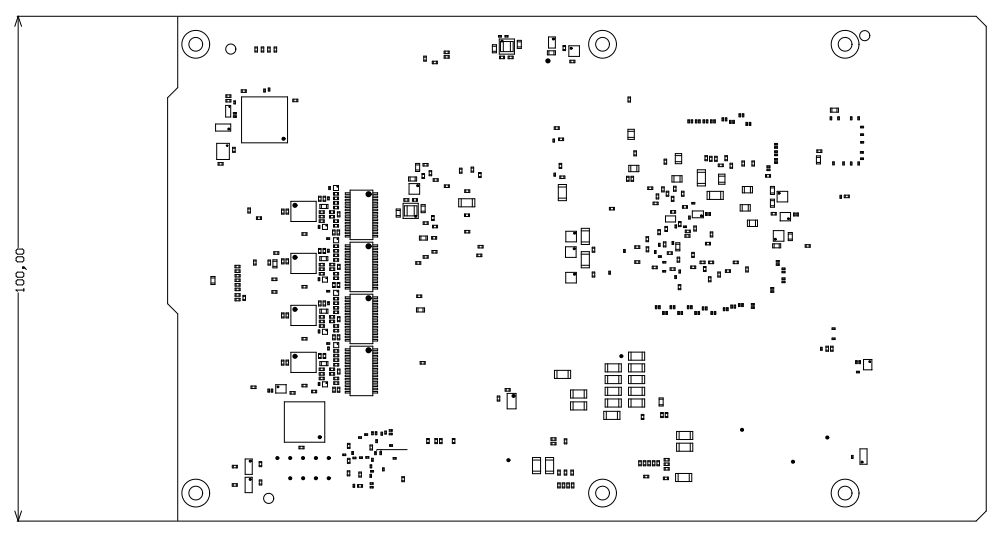
Figure 25: Physical dimensions drawing
Variants Currently In Production
| Trenz shop TE0xxx overview page | |
|---|---|
| English page | German page |
Table 32: Shop Overview
Revision History
Hardware Revision History
| Date | Revision | Notes | PCN | Documentation Link |
|---|---|---|---|---|
| - | 02 | current available board revision | - | TEC0850-02 |
| - | 01 | Prototypes | - | - |
Table 33: Module hardware revision history
Document Change History
| Date | Revision | Constributor | Description |
|---|---|---|---|
| |||
-- | all |
|
Table 34: Document change history
Disclaimer
Data Privacy
Please also note our data protection declaration at https://www.trenz-electronic.de/en/Data-protection-Privacy
Document Warranty
The material contained in this document is provided “as is” and is subject to being changed at any time without notice. Trenz Electronic does not warrant the accuracy and completeness of the materials in this document. Further, to the maximum extent permitted by applicable law, Trenz Electronic disclaims all warranties, either express or implied, with regard to this document and any information contained herein, including but not limited to the implied warranties of merchantability, fitness for a particular purpose or non infringement of intellectual property. Trenz Electronic shall not be liable for errors or for incidental or consequential damages in connection with the furnishing, use, or performance of this document or of any information contained herein.
Limitation of Liability
In no event will Trenz Electronic, its suppliers, or other third parties mentioned in this document be liable for any damages whatsoever (including, without limitation, those resulting from lost profits, lost data or business interruption) arising out of the use, inability to use, or the results of use of this document, any documents linked to this document, or the materials or information contained at any or all such documents. If your use of the materials or information from this document results in the need for servicing, repair or correction of equipment or data, you assume all costs thereof.
Copyright Notice
No part of this manual may be reproduced in any form or by any means (including electronic storage and retrieval or translation into a foreign language) without prior agreement and written consent from Trenz Electronic.
Technology Licenses
The hardware / firmware / software described in this document are furnished under a license and may be used /modified / copied only in accordance with the terms of such license.
Environmental Protection
To confront directly with the responsibility toward the environment, the global community and eventually also oneself. Such a resolution should be integral part not only of everybody's life. Also enterprises shall be conscious of their social responsibility and contribute to the preservation of our common living space. That is why Trenz Electronic invests in the protection of our Environment.
REACH, RoHS and WEEE
REACH
Trenz Electronic is a manufacturer and a distributor of electronic products. It is therefore a so called downstream user in the sense of REACH. The products we supply to you are solely non-chemical products (goods). Moreover and under normal and reasonably foreseeable circumstances of application, the goods supplied to you shall not release any substance. For that, Trenz Electronic is obliged to neither register nor to provide safety data sheet. According to present knowledge and to best of our knowledge, no SVHC (Substances of Very High Concern) on the Candidate List are contained in our products. Furthermore, we will immediately and unsolicited inform our customers in compliance with REACH - Article 33 if any substance present in our goods (above a concentration of 0,1 % weight by weight) will be classified as SVHC by the European Chemicals Agency (ECHA).
RoHS
Trenz Electronic GmbH herewith declares that all its products are developed, manufactured and distributed RoHS compliant.
WEEE
Information for users within the European Union in accordance with Directive 2002/96/EC of the European Parliament and of the Council of 27 January 2003 on waste electrical and electronic equipment (WEEE).
Users of electrical and electronic equipment in private households are required not to dispose of waste electrical and electronic equipment as unsorted municipal waste and to collect such waste electrical and electronic equipment separately. By the 13 August 2005, Member States shall have ensured that systems are set up allowing final holders and distributors to return waste electrical and electronic equipment at least free of charge. Member States shall ensure the availability and accessibility of the necessary collection facilities. Separate collection is the precondition to ensure specific treatment and recycling of waste electrical and electronic equipment and is necessary to achieve the chosen level of protection of human health and the environment in the European Union. Consumers have to actively contribute to the success of such collection and the return of waste electrical and electronic equipment. Presence of hazardous substances in electrical and electronic equipment results in potential effects on the environment and human health. The symbol consisting of the crossed-out wheeled bin indicates separate collection for waste electrical and electronic equipment.
Trenz Electronic is registered under WEEE-Reg.-Nr. DE97922676.
Overview
Content Tools